


All products are subject to strict incoming inspection and quality control procedures.
We ensure part authenticity, correct specifications, and reliable performance through standardized testing and continuous process improvement.
Quality Warranty
All Categories
-
Integrated Circuits (ICs)
Integrated Circuits (ICs)
- Interface - Sensor, Capacitive Touch(642)
- Specialized ICs(12302)
- Power Management (PMIC) - Special Purpose Regulators(5644)
- Power Management (PMIC) - Voltage Regulators - Linear Regulator Controllers(793)
- Power Management (PMIC) - Voltage Regulators - Linear + Switching(1829)
- Power Management (PMIC) - Voltage Regulators - Linear, Low Drop Out (LDO) Regulators(70981)
- Power Management (PMIC) - Voltage Regulators - DC DC Switching Regulators(39569)
- Power Management (PMIC) - DC DC Switching Controllers(13507)
- Power Management (PMIC) - Voltage Reference(9453)
- Power Management (PMIC) - V/F and F/V Converters(145)
- Power Management (PMIC) - Thermal Management(592)
- Power Management (PMIC) - Supervisors(47946)
- Power Management (PMIC) - RMS to DC Converters(170)
- Power Management (PMIC) - Power Supply Controllers, Monitors(2104)
- Power Management (PMIC) - Power Over Ethernet (PoE) Controllers(1008)
- Power Management (PMIC) - Power Management - Specialized(7722)
- Power Management (PMIC) - Power Distribution Switches, Load Drivers(7706)
- Power Management (PMIC) - PFC (Power Factor Correction)(1222)
- Power Management (PMIC) - OR Controllers, Ideal Diodes(705)
- Power Management (PMIC) - Motor Drivers, Controllers(4712)
- Power Management (PMIC) - Lighting, Ballast Controllers(560)
- Power Management (PMIC) - LED Drivers(7282)
- Power Management (PMIC) - Laser Drivers(573)
- Power Management (PMIC) - Hot Swap Controllers(2816)
- Power Management (PMIC) - Gate Drivers(7083)
- Power Management (PMIC) - Full Half-Bridge (H Bridge) Drivers(1342)
- Power Management (PMIC) - Energy Metering(654)
- Power Management (PMIC) - Display Drivers(1435)
- Power Management (PMIC) - Current Regulation/Management(1481)
- Power Management (PMIC) - Battery Management(5553)
- Power Management (PMIC) - Battery Chargers(3831)
- Power Management (PMIC) - AC DC Converters, Offline Switchers(4905)
- Memory - Controllers(358)
- Memory - Configuration PROMs for FPGAs(639)
- Memory - Batteries(13)
- Memory - Memory(65694)
- Logic - Universal Bus Functions(706)
- Logic - Translators, Level Shifters(2854)
- Logic - Specialty Logic(1870)
- Logic - Signal Switches, Multiplexers, Decoders(9420)
- Logic - Shift Registers(2665)
- Logic - Parity Generators and Checkers(335)
- Logic - Multivibrators(831)
- Logic - Latches(3658)
- Logic - Gates and Inverters - Multi-Function, Configurable(1687)
- Logic - Gates and Inverters(16453)
- Logic - Flip Flops(7780)
- Logic - FIFOs Memory(4240)
- Logic - Counters, Dividers(3456)
- Logic - Comparators(592)
- Logic - Buffers, Drivers, Receivers, Transceivers(17835)
- Linear - Video Processing(2909)
- Linear - Comparators(5084)
- Linear - Analog Multipliers, Dividers(263)
- Linear - Amplifiers - Video Amps and Modules(1905)
- Linear - Amplifiers - Special Purpose(1856)
- Linear - Amplifiers - Instrumentation, OP Amps, Buffer Amps(34236)
- Linear - Amplifiers - Audio(4567)
- Interface - Voice Record and Playback(556)
- Interface - UARTs (Universal Asynchronous Receiver Transmitter)(1237)
- Interface - Telecom(4467)
- Interface - Specialized(4833)
- Interface - Signal Terminators(333)
- Interface - Signal Buffers, Repeaters, Splitters(1449)
- Interface - Serializers, Deserializers(1480)
- Interface - Sensor and Detector Interfaces(1524)
- Interface - Modules(169)
- Interface - Modems - ICs and Modules(407)
- Interface - I/O Expanders(1136)
- Interface - Filters - Active(1226)
- Interface - Encoders, Decoders, Converters(714)
- Interface - Drivers, Receivers, Transceivers(20755)
- Interface - Direct Digital Synthesis (DDS)(117)
- Interface - Controllers(3628)
- Interface - CODECS(1676)
- Interface - Analog Switches, Multiplexers, Demultiplexers(12567)
- Interface - Analog Switches - Special Purpose(2533)
- Embedded - System On Chip (SoC)(4496)
- Embedded - PLDs (Programmable Logic Device)(971)
- Embedded - Microprocessors(10083)
- Embedded - Application Specific Microcontrollers(2275)
- Embedded - Microcontrollers(99285)
- Embedded - Microcontrollers, Microprocessor, FPGA Modules(1527)
- Embedded - FPGAs (Field Programmable Gate Array) with Microcontrollers(81)
- Embedded - FPGAs (Field Programmable Gate Array)(27747)
- Embedded - DSP (Digital Signal Processors)(4081)
- Embedded - CPLDs (Complex Programmable Logic Devices)(5187)
- Data Acquisition - Touch Screen Controllers(1210)
- Data Acquisition - Digital to Analog Converters (DAC)(14419)
- Data Acquisition - Digital Potentiometers(6250)
- Data Acquisition - Analog to Digital Converters (ADC)(17776)
- Data Acquisition - Analog Front End (AFE)(787)
- Data Acquisition - ADCs/DACs - Special Purpose(3043)
- Clock/Timing - Real Time Clocks(2446)
- Clock/Timing - Programmable Timers and Oscillators(23469)
- Clock/Timing - IC Batteries(4)
- Clock/Timing - Delay Lines(1049)
- Clock/Timing - Clock Generators, PLLs, Frequency Synthesizers(32775)
- Clock/Timing - Clock Buffers, Drivers(4568)
- Clock/Timing - Application Specific Clock/Timing(8652)
- Audio Special Purpose(1564)
Relevant Manufacturer


-
Discrete Semiconductor Products
Discrete Semiconductor Products
- Current Regulation - Diodes, Transistors(1090)
- Transistors - Special Purpose(226)
- Transistors - Programmable Unijunction(48)
- Transistors - JFETs(1558)
- Transistors - IGBTs - Single(4799)
- Transistors - IGBTs - Modules(63420)
- Transistors - IGBTs - Arrays(26)
- Transistors - FETs, MOSFETs - Single(48330)
- Transistors - FETs, MOSFETs - RF(4903)
- Transistors - FETs, MOSFETs - Arrays(6641)
- Transistors - Bipolar (BJT) - Single, Pre-Biased(4539)
- Transistors - Bipolar (BJT) - Single(25800)
- Transistors - Bipolar (BJT) - RF(2087)
- Transistors - Bipolar (BJT) - Arrays, Pre-Biased(2115)
- Transistors - Bipolar (BJT) - Arrays(2310)
- Thyristors - TRIACs(4044)
- Thyristors - SCRs - Modules(3967)
- Thyristors - SCRs(5436)
- Thyristors - DIACs, SIDACs(319)
- Power Driver Modules(1627)
- Diodes - Zener - Single(87483)
- Diodes - Zener - Arrays(2619)
- Diodes - Variable Capacitance (Varicaps, Varactors)(1200)
- Diodes - RF Diodes(2753)
- Diodes - Rectifiers - Single(67528)
- Diodes - Rectifiers - Arrays(20581)
- Diodes - Bridge Rectifiers(11700)
Relevant Manufacturer


-
RF and Wireless
RF and Wireless
- Subscriber Identification Module (SIM) Cards(77)
- RF Circulators and Isolators(1742)
- RFID, RF Access, Monitoring ICs(1550)
- RFID Transponders, Tags(747)
- RFID Reader Modules(464)
- RFID Evaluation and Development Kits, Boards(30)
- RFID Antennas(329)
- RFI and EMI - Shielding and Absorbing Materials(6444)
- RFI and EMI - Contacts, Fingerstock and Gaskets(7497)
- RF Transmitters(668)
- RF Transceiver Modules and Modems(6900)
- RF Transceiver ICs(4169)
- RF Switches(9276)
- RF Shields(16401)
- RF Receivers(1998)
- RF Receiver, Transmitter, and Transceiver Finished Units(2763)
- RF Power Dividers/Splitters(1223)
- RF Power Controller ICs(86)
- RF Modulators(710)
- RF Mixers(2800)
- RF Misc ICs and Modules(3276)
- RF Front End (LNA + PA)(419)
- RF Evaluation and Development Kits, Boards(747)
- RF Directional Coupler(2718)
- RF Multiplexers(1464)
- RF Detectors(412)
- RF Demodulators(249)
- RF Antennas(12319)
- RF Amplifiers(19651)
- Balun(1496)
- Attenuators(4852)
Relevant Manufacturer


-
Optoelectronics
Optoelectronics
- Optomechanical(480)
- Lighting Fixtures(125)
- Laser Diodes, Laser Modules - Laser Delivery, Laser Fibers(345)
- HeNe Laser Systems(31)
- HeNe Laser Heads(27)
- Display Backlights(93)
- Xenon Lighting(387)
- Touch Screen Overlays(453)
- Panel Indicators, Pilot Lights(75729)
- Remote Phosphor Light Source(269)
- Reflectors(665)
- Light Pipes(5384)
- Lenses(4951)
- Spacers, Standoffs(2718)
- Lamp Replacements(29718)
- Circuit Board Indicators, Arrays, Light Bars, Bar Graphs(9083)
- LED Thermal Products(667)
- LED Lighting Kits(64)
- LED White Lighting(37580)
- LED Color Lighting(4728)
- LED COBs, Engines, Modules, Strips(28735)
- LED Indication - Discrete(27601)
- Laser Diodes, Modules(1553)
- Incandescent, Neon Lamps(311004)
- Cold Cathode Fluorescent (CCFL) & UV Lamps(164)
- Ballasts, Inverters(7728)
- LED Emitters - Infrared, UV, Visible(3871)
- Fiber Optic Transmitters - Drive Circuitry Integrated(4085)
- Fiber Optic Transmitters - Discrete(350)
- Fiber Optic Transceiver Modules(18758)
- Fiber Optic Switches, Multiplexers, Demultiplexers(1387)
- Fiber Optic Receivers(695)
- Fiber Optic Attenuators(654)
- Electroluminescent(102)
- Display, Monitor - LCD Driver/Controller(98)
- Vacuum Fluorescent (VFD)(249)
- LED Dot Matrix and Cluster(865)
- LED Character and Numeric(5421)
- LCD, OLED, Graphic(4654)
- LCD, OLED Character and Numeric(2202)
- Display Bezels, Lenses(88)
- LED Addressable, Specialty(458)
Relevant Manufacturer


-
Sensors, Transducers
Sensors, Transducers
- Industrial Sensors - Ultrasonic Receivers, Transmitters - Industrial(115)
- Industrial Sensors - Thermostats - Mechanical - Industrial(3103)
- Industrial Sensors - Temperature Sensors - Analog and Digital Output - Industrial(209)
- Industrial Sensors - Proximity Sensors - Industrial(13611)
- Industrial Sensors - Pressure Sensors, Transducers - Industrial(26503)
- Optical Sensors - Photonics - Counters, Detectors, SPCM (Single Photon Counting Module)(751)
- Optical Sensors - Camera Modules(875)
- Industrial Sensors - Position, Proximity, Speed (Modules) - Industrial(554)
- Industrial Sensors - Force Sensors, Load Cells - Industrial(346)
- Industrial Sensors - Flow Sensors - Industrial(151)
- Industrial Sensors - Float, Level Sensors - Industrial(310)
- Industrial Sensors - Encoders - Industrial(4980)
- Industrial Sensors - Color Sensors - Industrial(50)
- Touch Sensors(100)
- Ultrasonic Receivers, Transmitters(2421)
- Temperature Sensors - Thermostats - Solid State(1096)
- Temperature Sensors - Thermostats - Mechanical(3397)
- Temperature Sensors - Thermocouples, Temperature Probes(1921)
- Temperature Sensors - RTD (Resistance Temperature Detector)(1525)
- Temperature Sensors - PTC Thermistors(2273)
- Temperature Sensors - NTC Thermistors(13259)
- Temperature Sensors - Analog and Digital Output(3928)
- Strain Gauges(1399)
- Specialized Sensors(1861)
- Solar Cells(503)
- Shock Sensors(84)
- Sensor Interface - Junction Blocks(2519)
- Sensor Cable - Assemblies(22011)
- Proximity/Occupancy Sensors - Finished Units(725)
- Proximity Sensors(2860)
- Pressure Sensors, Transducers(11317)
- Position Sensors - Angle, Linear Position Measuring(6022)
- Optical Sensors - Reflective - Logic Output(194)
- Optical Sensors - Reflective - Analog Output(432)
- Optical Sensors - Phototransistors(1027)
- Optical Sensors - Photointerrupters - Slot Type - Transistor Output(1427)
- Optical Sensors - Photointerrupters - Slot Type - Logic Output(1215)
- Industrial Sensors - Photoelectric, Industrial(16763)
- Optical Sensors - Photodiodes(1543)
- Optical Sensors - Photo Detectors - Remote Receiver(2605)
- Optical Sensors - Photo Detectors - Logic Output(146)
- Optical Sensors - Photo Detectors - CdS Cells(74)
- Optical Sensors - Distance Measuring(377)
- Optical Sensors - Ambient Light, IR, UV Sensors(1305)
- Multifunction(558)
- Motion Sensors - Vibration Sensors(337)
- Motion Sensors - Tilt Switches(67)
- Motion Sensors - Optical Motion Sensors(719)
- Motion Sensors - Inclinometers(175)
- Motion Sensors - IMUs (Inertial Measurement Units)(416)
- Motion Sensors - Gyroscopes(214)
- Motion Sensors - Accelerometers(1911)
- Magnets - Sensor Matched Magnets(119)
- Magnets - Multi Purpose Magnets(1965)
- Magnetic Sensors - Switches (Solid State)(3700)
- Magnetic Sensors - Position, Proximity, Speed (Modules)(5199)
- Magnetic Sensors - Linear, Compass (ICs)(1247)
- Magnetic Sensors - Compass, Magnetic Field (Modules)(35)
- LVDT Transducers (Linear Variable Differential Transformer)(204)
- IrDA Transceiver Modules(196)
- Optical Sensors - Image Sensors, Camera(2235)
- Humidity, Moisture Sensors(1425)
- Gas Sensors(1217)
- Force Sensors, Load Cells(188)
- Flow Sensors(550)
- Float, Level Sensors(1343)
- Encoders(6357)
- Particle, Dust Sensors(43)
- Current Sensors(3455)
- Color Sensors(85)
- Sensor, Transducer Amplifiers(1905)
Relevant Manufacturer


-
Connectors, Interconnects
Connectors, Interconnects
- USB, DVI, HDMI Connectors(446)
- Solid State Lighting Connectors(555)
- Sockets for ICs, Transistors(953)
- Pluggable Connectors(1221)
- Photovoltaic (Solar Panel) Connectors(136)
- Fiber Optic Connectors(370)
- FFC, FPC (Flat Flexible) Connectors(761)
- D-Sub, D-Shaped Connectors(2887)
- Coaxial Connectors (RF)(2389)
- Circular Connectors(14162)
- Blade Type Power Connectors(273)
- AC Power Connectors - Plugs and Receptacles(2597)
- USB, DVI, HDMI Connectors - USB, DVI, HDMI Connector Adapters(572)
- USB, DVI, HDMI Connectors - USB, DVI, HDMI Connector Assemblies(4298)
- Terminals - Wire to Board Connectors(217)
- Terminals - Wire Splice Connectors(4322)
- Terminals - Wire Pin Connectors(328)
- Terminals - Turret Connectors(1273)
- Terminals - Specialized Connectors(2042)
- Terminals - Spade Connectors(3902)
- Terminals - Solder Lug Connectors(345)
- Terminals - Screw Connectors(745)
- Terminals - Ring Connectors(12596)
- Terminals - Lugs(4747)
- Terminals - Quick Connects, Quick Disconnect Connectors(8514)
- Terminals - PC Pin, Single Post Connectors(3776)
- Terminals - PC Pin Receptacles, Socket Connectors(5883)
- Terminals - Magnetic Wire Connectors(1653)
- Terminals - Knife Connectors(112)
- Terminals - Housings, Boots(2850)
- Terminals - Foil Connectors(108)
- Terminals - Barrel, Bullet Connectors(1107)
- Terminals - Terminal Adapters(137)
- Terminal Strips and Turret Boards(1159)
- Terminal Junction Systems(2533)
- Terminal Blocks - Wire to Board(43615)
- Terminal Blocks - Specialized(3722)
- Terminal Blocks - Power Distribution(847)
- Terminal Blocks - Panel Mount(1359)
- Terminal Blocks - Interface Modules(1819)
- Terminal Blocks - Headers, Plugs and Sockets(119920)
- Terminal Blocks - Din Rail, Channel(9373)
- Terminal Blocks - Terminal Block Contacts(65)
- Terminal Blocks - Barrier Blocks(47517)
- Terminal Blocks - Terminal Block Adapters(1059)
- Solid State Lighting Connectors - Solid State Lighting Connector Contacts(271)
- Solid State Lighting Connectors - Solid State Lighting Connector Assemblies(1344)
- Sockets for ICs, Transistors - Socket Adapters(275)
- Sockets for ICs, Transistors - IC Sockets(22148)
- Shunts, Jumpers(907)
- Rectangular Connectors - Spring Loaded(7721)
- Rectangular Connectors - Rectangular Connector Housings(43023)
- Rectangular Connectors - Headers, Specialty Pin(6129)
- Rectangular Connectors - Headers, Receptacles, Female Sockets(229601)
- Rectangular Connectors - Headers, Male Pins(543338)
- Rectangular Connectors - Free Hanging, Panel Mount(30142)
- Rectangular Connectors - Rectangular Connector Contacts(10681)
- Rectangular Connectors - Board In, Direct Wire to Board(2432)
- Rectangular Connectors - Rectangular Connector Adapters(475)
- Rectangular - Board to Board Connectors - Headers, Receptacles, Female Sockets(9)
- Rectangular - Board to Board Connectors - Headers, Male Pins(2)
- Rectangular Connectors - Board Spacers, Stackers (Board to Board)(238901)
- Rectangular Connectors - Arrays, Edge Type, Mezzanine (Board to Board)(37853)
- AC Power Connectors - Power Entry Modules (PEM)(10310)
- Pluggable Connectors - Pluggable Connector Assemblies(6049)
- Photovoltaic (Solar Panel) Connectors - Photovoltaic (Solar Panel) Connector Contacts(77)
- Photovoltaic (Solar Panel) Connectors - Photovoltaic (Solar Panel) Connector Assemblies(504)
- Modular/Ethernet Connectors - Modular/Ethernet Connector Wiring Blocks(99)
- Modular/Ethernet Connectors - Modular/Ethernet Connector (RJ45, RJ11) Plugs(1674)
- Modular/Ethernet Connectors - Modular/Ethernet Connector Plug Housings(181)
- Modular/Ethernet Connectors - Modular/Ethernet Connector (RJ45) Jacks With Magnetics(10152)
- Modular/Ethernet Connectors - Modular/Ethernet Connector (RJ45, RJ11) Jacks(23416)
- Modular/Ethernet Connectors - Modular/Ethernet Connector Adapters(855)
- Memory Connectors - PC Cards - Adapters(21)
- Memory Connectors - PC Card Sockets(3299)
- Memory Connectors - Inline Module Sockets(3390)
- LGH Connectors(764)
- Keystone Connectors - Keystone Inserts(2758)
- Keystone Connectors - Keystone Faceplates, Frames(1926)
- Heavy Duty Connectors - Heavy Duty Connector Inserts, Modules(4190)
- Heavy Duty Connectors - Heavy Duty Connector Housings, Hoods, Bases(17226)
- Heavy Duty Connectors - Heavy Duty Connector Frames(523)
- Heavy Duty Connectors - Heavy Duty Connector Contacts(1832)
- Heavy Duty Connectors - Heavy Duty Connector Assemblies(671)
- Fiber Optic Connectors - Fiber Optic Connector Housings(919)
- Fiber Optic Connectors - Fiber Optic Connector Adapters(4455)
- Fiber Optic Connectors - Fiber Optic Connector Assemblies(3001)
- FFC, FPC (Flat Flexible) Connectors - FFC, FPC (Flat Flexible) Connector Housings(652)
- FFC, FPC (Flat Flexible) Connectors - FFC, FPC (Flat Flexible) Connector Contacts(202)
- FFC, FPC (Flat Flexible) Connectors - FFC, FPC (Flat Flexible) Connector Assemblies(18691)
- D-Sub, D-Shaped Connectors - D-Sub, D-Shaped Connector Terminators(47)
- D-Sub, D-Shaped Connectors - D-Sub, D-Shaped Connector Housings(12238)
- D-Sub, D-Shaped Connectors - D-Sub, D-Shaped Connector Contacts(2714)
- D-Sub, D-Shaped Connectors - D-Sub, D-Shaped Connector Backshells, Hoods(5995)
- D-Sub, D-Shaped Connectors - D-Sub, D-Shaped Connector Adapters(1304)
- D-Sub, D-Shaped Connectors - D-Sub Connector Assemblies(141346)
- D-Sub, D-Shaped Connectors - Centronics Connectors(8770)
- Contacts - Contacts, Spring Loaded (Pogo Pins), and Pressure(630)
- Contacts - Multi Purpose(6196)
- Contacts - Leadframe(122)
- Coaxial Connectors (RF) - Coaxial Connector (RF) Terminators(1231)
- Coaxial Connectors (RF) - Coaxial Connector (RF) Contacts(480)
- Coaxial Connectors (RF) - Coaxial Connector (RF) Adapters(6386)
- Coaxial Connectors (RF) - Coaxial Connector (RF) Assemblies(25734)
- Circular Connectors - Circular Connector Housings(441226)
- Circular Connectors - Circular Connector Contacts(4737)
- Circular Connectors - Backshells and Cable Clamps(53692)
- Circular Connectors - Circular Connector Adapters(8839)
- Circular Connectors - Circular Connector Assemblies(1196254)
- Card Edge Connectors - Card Edge Connector Housings(469)
- Card Edge Connectors - Edgeboard Connectors(672683)
- Card Edge Connectors - Card Edge Connector Contacts(325)
- Card Edge Connectors - Card Edge Connector Adapters(73)
- Blade Type Power Connectors - Blade Type Power Connector Housings(837)
- Blade Type Power Connectors - Blade Type Power Connector Contacts(393)
- Blade Type Power Connectors - Blade Type Power Connector Assemblies(4163)
- Between Series Adapters(649)
- Barrel Connectors - Power Connectors(935)
- Barrel Connectors - Audio Connectors(2432)
- Barrel Connectors - Barrel Connector Adapters(92)
- Banana and Tip Connectors - Jacks, Plugs(1644)
- Banana and Tip Connectors - Binding Posts(239)
- Banana and Tip Connectors - Banana and Tip Connector Adapters(75)
- Backplane Connectors - Specialized(45586)
- Backplane Connectors - Backplane Connector Housings(6863)
- Backplane Connectors - Hard Metric, Standard(6297)
- Backplane Connectors - DIN 41612(9408)
- Backplane Connectors - Backplane Connector Contacts(3583)
- Backplane Connectors - ARINC Inserts(2357)
- Backplane Connectors - ARINC(3789)
Relevant Manufacturer


-
Resistors
-
Capacitors
Capacitors
- Aluminum Capacitors(16817)
- Trimmers, Variable Capacitors(3151)
- Thin Film Capacitors(3473)
- Tantalum Capacitors(136103)
- Tantalum - Polymer Capacitors(9778)
- Silicon Capacitors(320)
- Niobium Oxide Capacitors(330)
- Mica and PTFE Capacitors(9101)
- Film Capacitors(150406)
- Electric Double Layer Capacitors (EDLC), Supercapacitors(2782)
- Ceramic Capacitors(833829)
- Capacitor Networks, Arrays(2383)
- Aluminum Electrolytic Capacitors(125325)
- Aluminum - Polymer Capacitors(7544)
Relevant Manufacturer


-
Transformers
-
Isolators
Isolators
Relevant Manufacturer


-
Crystals, Oscillators, Resonators
-
Switches
Switches
- Interlock Switches(2893)
- Emergency Stop (E-Stop) Switches(1160)
- Cable Pull Switches(571)
- Toggle Switches(33608)
- Thumbwheel Switches(742)
- Tactile Switches(14263)
- Limit Switches(28077)
- Slide Switches(5166)
- Selector Switches(9720)
- Rotary Switches(13850)
- Rocker Switches(53790)
- Pushbutton Switches - Hall Effect(127)
- Pushbutton Switches(190826)
- Programmable Display Switches(39)
- Navigation Switches, Joystick(1882)
- Magnetic, Reed Switches(1399)
- Keypad Switches(637)
- Keylock Switches(3684)
- DIP Switches(7747)
- Configurable Switch Components - Configurable Switch Lens(1435)
- Configurable Switch Components - Configurable Switch Illumination Sources(1236)
- Configurable Switch Components - Configurable Switch Contact Blocks(1401)
- Configurable Switch Components - Configurable Switch Bodies(16077)
- Disconnect Switch Components(2567)
Relevant Manufacturer


-
Relays
Relays
- Safety Relays(1310)
- Reed Relays(1735)
- High Frequency (RF) Relays(1190)
- Contactors (Solid State)(686)
- Contactors (Electromechanical)(11952)
- Automotive Relays(1881)
- Solid State Relays (SSR)(10652)
- Signal Relays, Up to 2 Amps(9149)
- Relay Sockets(2075)
- Power Relays, Over 2 Amps(31604)
- I/O Relay Modules(712)
- I/O Relay Modules - Input(2)
- I/O Relay Module Racks(247)
Relevant Manufacturer


Select Language
Current Language
English
- English
- Deutsch
- Italia
- Français
- 日本語
- 한국의
- русский
- Svenska
- Nederland
- español
- Português
- polski
- Suomi
- Gaeilge
- Slovenská
- Slovenija
- Čeština
- Melayu
- Magyarország
- Hrvatska
- Dansk
- românesc
- Indonesia
- Ελλάδα
- Български език
- Afrikaans
- IsiXhosa
- isiZulu
- lietuvių
- Maori
- Kongeriket
- Монголулс
- O'zbek
- Tiếng Việt
- हिंदी
- اردو
- Kurdî
- Català
- Bosna
- Euskera
- العربية
- فارسی
- Corsa
- Chicheŵa
- עִבְרִית
- Latviešu
- Hausa
- Беларусь
- አማርኛ
- Republika e Shqipërisë
- Eesti Vabariik
- íslenska
- မြန်မာ
- Македонски
- Lëtzebuergesch
- საქართველო
- Cambodia
- Pilipino
- Azərbaycan
- ພາສາລາວ
- বাংলা ভাষার
- پښتو
- malaɡasʲ
- Кыргыз тили
- Ayiti
- Қазақша
- Samoa
- සිංහල
- ภาษาไทย
- Україна
- Kiswahili
- Cрпски
- Galego
- नेपाली
- Sesotho
- Тоҷикӣ
- Türk dili
- ગુજરાતી
- ಕನ್ನಡkannaḍa
- मराठी
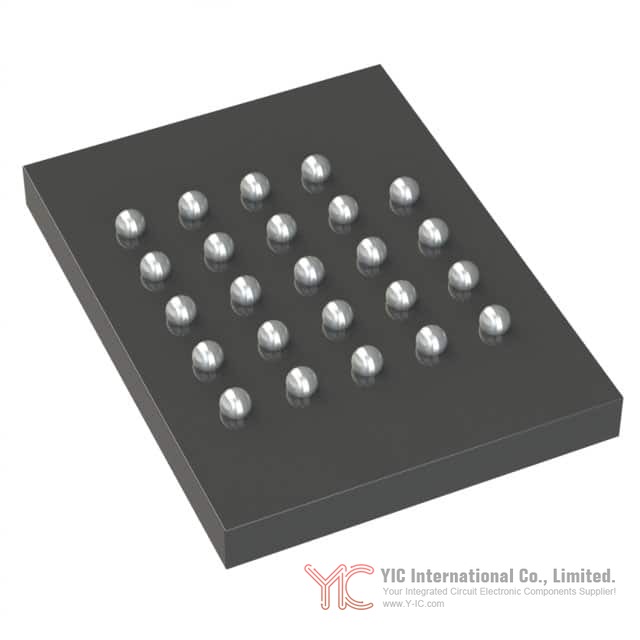
Image may be representation.
See specs for product details.
See specs for product details.
Infineon Technologies S25FL256LDPBHV020
| Part Number: | S25FL256LDPBHV020 |
|---|---|
| Manufacturer/Brand: | Cypress Semiconductor (Infineon Technologies) |
| Part of Description: | IC FLASH 256MBIT SPI/QUAD 24BGA |
| Datasheets: |
|
| RoHs Status: | ROHS3 Compliant |
| Payment: | PayPal / Credit Card / T/T |
| Shipment Way: | DHL / Fedex / TNT / UPS / EMS |
| Share: |
Ship From: Hong Kong
| Quantity | Unit Price |
|---|---|
| 3380+ | $4.9213 |
Online RFQ submissions: Fast responses, Better prices!
- Specifications
- Shopping Manual
- Shipping Information
- QC & Packaging
-
Infineon Technologies S25FL256LDPBHV020 technical specifications, attributes, parameters and parts with similar specifications to Infineon Technologies S25FL256LDPBHV020.Product Attribute Attribute Value Write Cycle Time - Word, Page - Voltage - Supply 2.7V ~ 3.6V Technology FLASH - NOR Supplier Device Package 24-BGA (8x6) Series FL-L Package / Case 24-TBGA Package Tray Operating Temperature -40°C ~ 105°C (TA) Product Attribute Attribute Value Mounting Type Surface Mount Memory Type Non-Volatile Memory Size 256Mbit Memory Organization 32M x 8 Memory Interface SPI - Quad I/O, QPI Memory Format FLASH Clock Frequency 66 MHz Base Product Number S25FL256 -
- Returns Policy
-
Returns must be requested within 60 days of the invoice date and include:
- Original invoice number
- Photo of the parts
- Brief explanation or test report stating the reason for return
Returns will not be accepted after 60 days. Returned items must be in original packaging and resalable condition. Returns due to customer errors at the time of quote or purchase will not be accepted. Contact customer service for return authorization before shipping.
- How to Buy
-
We support both online and offline orders. For detailed guidance on the ordering process, please visit the following link:
https://www.Y-IC.com/RFQ-Quote.htm
If you encounter any issues, feel free to contact our customer service team for assistance.
- Payment
-
We accept the following payment methods:
- T/T in advance (bank transfer)
- Western Union
- Credit Card / Visa / Mastercard / PayPal
Please note that customers are responsible for shipping fees, bank charges, duties, and taxes.

-
- Delivery Period
- Packages will be scheduled for delivery within 1-2 days after all items have arrived at our warehouse. In-stock items will be shipped within 24 hours. The delivery time varies based on the shipping method and the destination.
- Shipping Tracking
- Once the components are delivered, the tracking number will be emailed to you immediately. You can also find the tracking number in your order history.
- Shipping Rate
-
Shipping rates are determined by the size, weight, and destination of the package. YIC provides competitive shipping options through leading carriers such as DHL, FedEx and UPS. Additionally, we offer the option for customers to use their own shipping accounts for direct billing.

-
Quality Control (QC)

Packaging
ESD antistatic protection.
All products are packaged in anti-static bags and shipped with ESD antistatic protection. The label on the external ESD packaging will include our company information: part number, brand, and quantity.
We inspect all goods prior to shipment to ensure they are in excellent condition and verify that the parts are new, original, and match the datasheet specifications. After confirming that everyting is in order,we securely package the items and ship them via global express.


S25FL256LDPBHV020 Product Details
Introduction to the S25FL256LDPBHV020 Product
The Infineon S25FL256LDPBHV020 is a 256 Mbit (32 MB) NOR Flash memory device featuring a Serial Peripheral Interface (SPI) with up to Quad I/O operation, housed in a space-efficient 24-ball BGA (6x8 mm) package. Fabricated using 65-nm floating gate technology, the S25FL256LDPBHV020 is part of the FL-L family of non-volatile memory devices, targeting embedded and mobile applications that demand high reliability, fast read access, flexible protection, and low pin-count interconnects.
This device addresses design needs such as code shadowing, execute-in-place (XIP), secure parameter storage, and re-programmable data storage. Its compatibility with legacy Infineon SPI families, support for both 24- and 32-bit addressing, and availability of industrial and automotive temperature grades make it especially suitable for industrial, automotive, networking, and consumer devices.
Main Features and System Architecture of the S25FL256LDPBHV020
The S25FL256LDPBHV020 features a floating gate NOR architecture and leverages a 65nm process for high endurance (minimum 100,000 Program/Erase cycles) and robust data retention (minimum 20 years). Key architectural highlights include:
SPI-compatible, with selectable 1-bit, 2-bit (dual), or 4-bit (quad) I/O commands
Double Data Rate (DDR) read option for enhanced bandwidth
Clock rates up to 133 MHz (SDR reads); up to 66 MHz DDR
Page programming buffer (up to 256 bytes per operation)
Flexible, uniform erase sizes (4KB sector, 32KB half-block, 64KB block, chip erase)
Multi-grade temperature options: up to Automotive AEC-Q100 Grade 1 (-40°C to +125°C)
Voltage supply: wide operating range 2.7 V to 3.6 V; supports CMOS logic levels
Package options include BGA, SOIC, and WSON for layout flexibility
These attributes combine to provide system designers with a low-power, high-performance flash solution—especially effective when minimizing signal count is a priority.
Communication Protocols and Functional Modes of the S25FL256LDPBHV020
One of the S25FL256LDPBHV020's strengths is support for multiple SPI protocol variants:
Standard single-bit SPI (1-1-1) for compatibility and simple interfacing
Dual and Quad Output, Dual/Quad I/O, and Quad Peripheral Interface (QPI) for increased throughput via fewer clock cycles per data unit
Double Data Rate (DDR) commands allow data transfers on both clock edges, maximizing bandwidth for real-time and XIP scenarios
Command protocols are flexible, with 24or 32-bit addressing, enabling use in large memory-mapped spaces
Backward-compatibility modes and JEDEC standard commands (including SFDP for discoverable parameters) help streamline migration from previous generations or competitive devices
The device supports various SPI clock polarity and phase modes (Modes 0 and 3), and it provides transition options between command set widths for both legacy and high-performance applications.
Memory Structure and Address Mapping of the S25FL256LDPBHV020
The S25FL256LDPBHV020 organizes memory into uniform erase units:
Main flash array divided into 64KB blocks, 32KB half-blocks, and 4KB sectors
Supports both 24-bit (up to 16MB addressing, for backward compatibility) and 32-bit addresses (up to 4GB address space), selectable via configuration registers or commands
Separate address spaces for unique device ID, JEDEC SFDP parameters, and dedicated Security Regions (1024 bytes, divided into four 256-byte locks)
Registers mapped into address space for configuration, protection, and device management functions
Through these mechanisms, the device grants granular control over where and how code/data is stored and protected, and delivers flexibility for mapping into diverse system topologies.
Security Measures and Data Protection Capabilities in S25FL256LDPBHV020
Security is integral to the S25FL256LDPBHV020, reflecting its use in code storage and secure embedded platforms:
Four independent 256-byte Security Regions, each individually lockable (OTP, password, or lock-down modes)
Robust array protection: Legacy Block Protection (contiguous array portion), Individual Block Lock (per block/sector), Pointer Region Protection (customized sector boundary via nonvolatile pointer)
Power Supply Lock-down, password-based access, and permanent region protection, selectable and mutually exclusive for robust anti-malicious reprogramming constraints
Status Register Protect bits control hardware and software protection, influencing register and configuration lock-downs
Additionally, program/erase operations are verified, and status registers track errors for field diagnostics and robust firmware design. Data retention ratings and detailed power-up sequencing ensure robustness in mission-critical uses.
Register Design and Protection Mechanisms in the S25FL256LDPBHV020
The S25FL256LDPBHV020's register infrastructure is highly flexible:
Status Registers (non-volatile and volatile): provide operation status, error flags, and hardware protection control
Configuration Registers (1, 2, 3; non-volatile and volatile): store interface settings, block lock status, output driver strength, default power-up/protection modes, read latency, and burst wrap options
Individual/Region Protection Register (IRP) and Protection Register (PR): manage secure region access—including OTP password, lock-down, and permanent protection selections
Robust write and read commands, including Write Enable/Disable gating, volatile/non-volatile register distinctions
Up to 64-bit passwords for protected access (secure operation, anti-overwrite, and anti-hacking strategies)
Security and block locks can be tied to power cycles for flexible boot-time state management
This architecture supports industrial security standards and enables multi-tiered approaches to configuration management and sensitive data protection, critical in automotive and IoT deployments.
Instruction Set and Integrated Algorithm Functionality of the S25FL256LDPBHV020
The S25FL256LDPBHV020 supports an extensive suite of JEDEC/JESD216 commands, such as:
Variable-width read protocols: normal, fast, dual I/O, quad I/O (with or without DDR), configurable latency for signal integrity and speed optimization
Multiple programming commands: page, quad page, and OTP region programming
Erase commands: sector (4KB), half-block (32KB), block (64KB), full chip erase
Multi-level suspend and resume for program/erase, optimizing system responsiveness (e.g., real-time code fetches during background updates)
Register access, block locking/unlocking, pointer region configuration, deep power-down, and multiple reset mechanisms
Unique device ID, JEDEC signature, and SFDP discovery reads
Achieving maximum bandwidth and lowest power consumption in embedded MCU and SoC environments calls for understanding these command options and when to apply them.
Available Packages and Pin Configurations for the S25FL256LDPBHV020
To fit various layout and industrial requirements, the S25FL256LDPBHV020 is available in several package options:
24-ball BGA (6x8mm, 4x6 or 5x5 ball grid)
16-pin SOIC (narrow and wide body; for S25FL128L)
8-lead WSON (5x6 or 6x8mm)
Pinout is optimized for SPI and multi-I/O protocols, with key signals including: SCK, SI/IO0, SO/IO1, WP#/IO2, IO3/RESET#, CS#, VCC, VSS, etc.
BGA packages offer PCB footprint compatibility with alternative devices and ease design migration
Several packages are automotive-grade qualified per AEC-Q100 and rated to -40°C to +125°C for use in harsh environments
Package selection should consider board space, thermal constraints, and assembly processes such as reflow or ultrasonic cleaning.
Electrical Characteristics, Timing Specifications, and Thermal Properties of the S25FL256LDPBHV020
Engineers can utilize the S25FL256LDPBHV020 across varied voltage and thermal regimes:
Single-supply voltage: 2.7 V to 3.6 V (CMOS-compatible)
Standby, active, and deep power-down current rated for battery-powered and energy-sensitive systems
SDR operation up to 133 MHz, DDR up to 66 MHz; precise timing diagrams and slew rate guidelines provided to maximize signal integrity
Robust power-up/power-down sequencing requirements for data integrity
Wide operating temperature ranges and clearly specified absolute maximum ratings for automotive and industrial reliability
Adjustable output driver strength via configuration register for optimally matching PCB impedance
Implementing the S25FL256LDPBHV020 in System Applications Design Insights and Engineering Scenarios
In embedded systems, the S25FL256LDPBHV020 directly supports:
Code shadowing: Loading boot or OS code into RAM at system power-up
Execute-In-Place (XIP): Direct code fetch and execution from flash, enabled via high I/O bandwidth SPI modes and configurable read latency
Secure boot: Storage for signed firmware, with programmable, password, and permanent locks on security regions, vital for anti-tampering and update assurance
Automotive ECUs: AEC-Q100 qualification, data retention in harsh conditions, and wide temperature ratings meet vehicle OEM specs
IoT and networking: Unique device ID for inventory/tracking and secure provisioning steps
System firmware design: Multiple suspend/resume and protection mechanisms allow firmware update without system downtime
Engineering logic and configuration choices—such as transitioning between 24/32-bit addressing, configuring protection through IRP/PR registers, or optimizing DDR timing via Data Learning Patterns—are central to achieving high reliability and performance in these applications.
Alternative or Substitute Models for the S25FL256LDPBHV020
For engineers seeking functional or footprint alternatives to the S25FL256LDPBHV020, Infineon's related FL-L series products are primary candidates:
S25FL128L: 128 Mbit (16 MB) variant, functionally similar but with reduced density; available in matching packages; compatible command set and footprint for density downsizing
Previous-generation compatible series: FL-S, FL1-K, FL-P (validate command and register subset for pin compatibility; see migration notes and device-specific datasheets)
For cross-brand design flexibility, devices supporting the JEDEC SPI, QPI, and SFDP standards—with equivalent density and footprint—can be considered, but should be carefully verified for timing, protection, and command set alignment
When substituting, confirm:
Addressing (24/32-bit) support and setup
Command protocol width (SPI, Dual, Quad, QPI) and performance (SDR, DDR)
Register and protection model compatibility (for secure and field-upgradable systems)
Package, pinout, and thermal capabilities suit the revised layout/environment
Conclusion
The Infineon S25FL256LDPBHV020 stands out as a versatile, robust 256Mb SPI/Quad NOR Flash memory device for demanding embedded applications. It combines industry-leading security features, comprehensive command and protection sets, flexible interface and addressing options, and broad package/temperature variants. Engineers and procurement specialists gain assurance of system reliability, code/data integrity, and migration flexibility within both industrial and automotive platforms. Thoughtful configuration and protection setup ensure that code and confidential parameters remain secure throughout the product lifecycle, making this device a compelling choice for modern embedded and connected systems.
Related Product

S25FL256LDPMFB000
S25FL256L - (32-MB), 3.0 V FL-L
S25FL256LDPBHN033
IC FLASH 256MBIT SPI/QUAD 24BGA
S25FL256LDPBHI023
IC FLASH 256MBIT SPI/QUAD 24BGA

S25FL256LDPMFI000
IC FLASH 256MBIT SPI/QUAD 16SOIC
S25FL256LDPBHV023
IC FLASH 256MBIT SPI/QUAD 24BGA
S25FL256LDPBHN020
IC FLASH 256MBIT SPI/QUAD 24BGA
S25FL256LDPMFB003
IC FLASH 256MBIT SPI/QUAD 16SOIC
S25FL256LDPMFB000
IC FLASH 256MBIT SPI/QUAD 16SOIC
S25FL256LDPBHI020
IC FLASH 256MBIT SPI/QUAD 24BGA
S25FL256LDPBHN023
IC FLASH 256MBIT SPI/QUAD 24BGA
S25FL256LDPBHI033
IC FLASH 256MBIT SPI/QUAD 24BGA
S25FL256LDPMFN000
IC FLASH 256MBIT SPI/QUAD 16SOIC
S25FL256LDPBHI030
IC FLASH 256MBIT SPI/QUAD 24BGA
S25FL256LDPMFI001
IC FLASH 256MBIT SPI/QUAD 16SOIC
S25FL256LDPBHN030
IC FLASH 256MBIT SPI/QUAD 24BGA
S25FL256LDPBHV033
IC FLASH 256MBIT SPI/QUAD 24BGA
S25FL256LDPBHV030
IC FLASH 256MBIT SPI/QUAD 24BGA
S25FL256LDPMFI003
IC FLASH 256MBIT SPI/QUAD 16SOIC
S25FL256LDPBHB023
IC FLASH 256MBIT SPI/QUAD 24BGA

S25FL256LDPBHI020Y
IC FLASH 256MBIT SPI/QUAD 24BGA
User Review
-
Geor***cott
Works fine as a signal component in timing circuits. No issues so far.May 12th, 2026
-
Oliv***arris
good communicationMay 8th, 2026
-
Bria***lson
Reliable FPGA. Worked smoothly in my MCU + signal integration project.April 28th, 2026
-
Jess***Miller
It works well in my FPGA signal processing setup. Performance is stable and meets the spec without issues so far.April 20th, 2026
-
Powe***sign_Guy
LM5145RGYR works fine in a DC-DC power design. Efficiency is good, but layout needs to be carefully optimized.April 17th, 2026
-
Powe***ive_
Used the FF900R12IP4 in an automotive inverter project. Power handling is solid and thermal performance is stable under load.April 8th, 2026
-
Vipe***rcuit
One unit failed during initial power-up, but the rest were fine. Mixed experience overall.March 31th, 2026
-
Hiro*** T.
Perfect replacement part. My system worked immediately after installation.March 23th, 2026
-
Yuki***
Works very well. I used AD8108ASTZ for video switching project. Stable and no noise problem.March 20th, 2026
-
Jaso***.
Used the AD8108ASTZ in a video routing board and it worked perfectly. Clean switching and no noticeable signal degradation.March 9th, 2026
-
Devo***.
Exactly as described. Great price for a pack of 10.March 4th, 2026
-
Alex***
Moderate quality chip. Works fine at room temperature, but in high temp conditions it seemed to drift. Not terrible, but not premium either.February 28th, 2026
-
Core***nalSourcing
Service was efficient and polite. Components were packed well and labels were clear. Appreciated the attention to detail.February 3th, 2026
-
Nano***icBuyer
Good.January 28th, 2026
-
Quan***Sourcing
Clear communication and quick updates during the whole process. The parts arrived as described. Very satisfied with the service.January 19th, 2026
-
Fusi***oreBuyer
Prompt replies. The order process was smooth and the delivery matched the promised timeline. Satisfied with the service.January 16th, 2026
-
Opti***pSolutions
GoodJanuary 9th, 2026
-
Tech***cuitBuyer
quick answer to our requestDecember 29th, 2025
-
Nova***ponentHub
Recommended, trustedDecember 25th, 2025
-
Grid***ion
Our procurement team relies on YIC for sourcing discontinued parts. They consistently deliver quality and handle cross-references when needed. Great value and support.December 17th, 2025
-
Terr***nse Microtech
Excellent service! We urgently needed a batch of TMS320LF2406APZA for a critical production line. YIC not only offered competitive pricing but also ensured on-time delivery. We’ll definitely reorder.December 10th, 2025
-
Tita***is Industrial
Our urgent production run was saved thanks to their stock of EOL components. Definitely a supplier we will use again.December 4th, 2025
-
Mich***_Embedded
Very professional supplier – confirmed stock quickly and kept me updated until delivery.November 25th, 2025
-
ches***_y
Our EMS line was waiting on MAX3030EEUE+T RS-422 drivers. IC-Components split the shipment—partial now, balance next week—so the SMT schedule didn’t slip. Practical and proactive.November 20th, 2025
-
ca_c***onents_ashley
The goods work as expected and the quote was clear. Only gripe: website showed ‘thousands in stock’ but true on-hand was zero; they turned it around via factory in 5 days and kept me posted. Fair recovery.November 11th, 2025
-
Quin***avis
Needed 250 pcs of LT4256-2IS8#PBF on short notice. They split reels for me, kept the MOQ reasonable, and sent full traceability docs + RoHS/REACH. Will buy again.November 3th, 2025
-
Jaso***ouis
Solid experience end to end. Order arrived faster than expected and the components came in moisture barrier bags with traceable labels.October 30th, 2025
-
AmpC***
The price is good, very satisfied with this purchase.October 22th, 2025
-
Eric***mmons
Great experience overall. The order was processed quickly, and the quality of the electronic components met our expectations.October 16th, 2025
-
Jona***n Brooks
Fast delivery and professional service. Great experience from order to receipt.October 9th, 2025
-
Jess***
Very professional supplier. I received my package quickly, and they were well packed. The team followed up until delivery was complete.September 28th, 2025
-
Sher***
Fast deliverySeptember 17th, 2025
-
Antw***Shawn
I found what I needed, great productSeptember 9th, 2025
-
Shir***neFrame
対応が良くて返信も早いです。発送も早くて助かりました。また買います。September 1th, 2025
-
7ama***
Seller was super nice, product quality is okay, and replies came really fast. Overall, shopping here felt easy and pleasant, would be happy to buy again.August 25th, 2025
-
Zinn***Clarke
Fast shipping, great customer service, and the item came super well-packed. Loved it!August 20th, 2025
-
Josh***Alexander
Outstanding customer support! They’re extremely helpful!July 3th, 2025
-
Lily***nchez
Everything is great!December 18th, 2024
-
Gabr*** Rivera
Great service! Fast shipping! Highly recommended!June 21th, 2023
-
Zoey***ice
The goods were delivered on time and well packaged. Communication with customer service was smooth and easy.April 27th, 2023
-
Madi*** Morgan
We're very satisfied with our purchasing experience at Y-IC, and we're glad to have Jimmy as our point of contact. He responds quickly and always provides competitive pricing.July 1th, 2022
-
Rile***eterson
We had a great experience, with excellent communication and customer support, competitive pricing, and fast delivery.March 4th, 2021
-
Anth*** Butler
I had an excellent experience with Y-IC. Their service was outstanding, and communication was always clear and friendly. All of my questions were answered promptly and professionally. Highly recommended!September 10th, 2020
-
Chlo***ughes
This is the fourth time I've purchased components from here. The quality and service are excellent! My contact is very responsive and highly professional!January 23th, 2020
0 Articles
Sign in to Comment
- Related Categories
- Featured Manufacturers
- Interface - Sensor, Capacitive Touch (642)Specialized ICs (12302)Power Management (PMIC) - Special Purpose Regulators (5644)Power Management (PMIC) - Voltage Regulators - Linear Regulator Controllers (793)Power Management (PMIC) - Voltage Regulators - Linear + Switching (1829)Power Management (PMIC) - Voltage Regulators - Linear, Low Drop Out (LDO) Regulators (70981)Power Management (PMIC) - Voltage Regulators - DC DC Switching Regulators (39569)Power Management (PMIC) - DC DC Switching Controllers (13507)Power Management (PMIC) - Voltage Reference (9453)Power Management (PMIC) - V/F and F/V Converters (145)Power Management (PMIC) - Thermal Management (592)Power Management (PMIC) - Supervisors (47946)


- Blogs & Posts
-
Google Acquires Raxium: What It Means for the Future of AR Glasses
Augmented reality (AR) is becoming a major part of the 2026 wearable AI race, with Google, Apple, and Meta competing to build smarter and more practic...May 21th, 2026
Choosing the Best Circuit Breaker for Your Electrical System
A circuit breaker is a safety device that automatically stops electrical current when a circuit becomes overloaded or a short circuit happens. Instead...May 20th, 2026
FT230X Pinout, Driver Setup, and Microcontroller Interfacing Guide
Modern computers usually use USB ports, but many microcontrollers and embedded devices still communicate through UART serial signals. This is where th...May 20th, 2026
Guide to DC-DC Converters Types and Power Conversion Topologies
DC-DC converters are electronic power circuits that change one DC voltage level into another DC voltage level. Many electronic devices and power syste...May 20th, 2026
Our Core Strength Our industry certifications & Advantages
S25FL256LDPBHV020Infineon Technologies |
Quantity*
|
Target Price(USD)
|