


All products are subject to strict incoming inspection and quality control procedures.
We ensure part authenticity, correct specifications, and reliable performance through standardized testing and continuous process improvement.
Quality Warranty
All Categories
-
Integrated Circuits (ICs)
Integrated Circuits (ICs)
- Interface - Sensor, Capacitive Touch(642)
- Specialized ICs(12302)
- Power Management (PMIC) - Special Purpose Regulators(5644)
- Power Management (PMIC) - Voltage Regulators - Linear Regulator Controllers(793)
- Power Management (PMIC) - Voltage Regulators - Linear + Switching(1829)
- Power Management (PMIC) - Voltage Regulators - Linear, Low Drop Out (LDO) Regulators(70981)
- Power Management (PMIC) - Voltage Regulators - DC DC Switching Regulators(39569)
- Power Management (PMIC) - DC DC Switching Controllers(13507)
- Power Management (PMIC) - Voltage Reference(9453)
- Power Management (PMIC) - V/F and F/V Converters(145)
- Power Management (PMIC) - Thermal Management(592)
- Power Management (PMIC) - Supervisors(47946)
- Power Management (PMIC) - RMS to DC Converters(170)
- Power Management (PMIC) - Power Supply Controllers, Monitors(2104)
- Power Management (PMIC) - Power Over Ethernet (PoE) Controllers(1008)
- Power Management (PMIC) - Power Management - Specialized(7722)
- Power Management (PMIC) - Power Distribution Switches, Load Drivers(7706)
- Power Management (PMIC) - PFC (Power Factor Correction)(1222)
- Power Management (PMIC) - OR Controllers, Ideal Diodes(705)
- Power Management (PMIC) - Motor Drivers, Controllers(4712)
- Power Management (PMIC) - Lighting, Ballast Controllers(560)
- Power Management (PMIC) - LED Drivers(7282)
- Power Management (PMIC) - Laser Drivers(573)
- Power Management (PMIC) - Hot Swap Controllers(2816)
- Power Management (PMIC) - Gate Drivers(7083)
- Power Management (PMIC) - Full Half-Bridge (H Bridge) Drivers(1342)
- Power Management (PMIC) - Energy Metering(654)
- Power Management (PMIC) - Display Drivers(1435)
- Power Management (PMIC) - Current Regulation/Management(1481)
- Power Management (PMIC) - Battery Management(5553)
- Power Management (PMIC) - Battery Chargers(3831)
- Power Management (PMIC) - AC DC Converters, Offline Switchers(4905)
- Memory - Controllers(358)
- Memory - Configuration PROMs for FPGAs(639)
- Memory - Batteries(13)
- Memory - Memory(65694)
- Logic - Universal Bus Functions(706)
- Logic - Translators, Level Shifters(2854)
- Logic - Specialty Logic(1870)
- Logic - Signal Switches, Multiplexers, Decoders(9420)
- Logic - Shift Registers(2665)
- Logic - Parity Generators and Checkers(335)
- Logic - Multivibrators(831)
- Logic - Latches(3658)
- Logic - Gates and Inverters - Multi-Function, Configurable(1687)
- Logic - Gates and Inverters(16453)
- Logic - Flip Flops(7780)
- Logic - FIFOs Memory(4240)
- Logic - Counters, Dividers(3456)
- Logic - Comparators(592)
- Logic - Buffers, Drivers, Receivers, Transceivers(17835)
- Linear - Video Processing(2909)
- Linear - Comparators(5084)
- Linear - Analog Multipliers, Dividers(263)
- Linear - Amplifiers - Video Amps and Modules(1905)
- Linear - Amplifiers - Special Purpose(1856)
- Linear - Amplifiers - Instrumentation, OP Amps, Buffer Amps(34236)
- Linear - Amplifiers - Audio(4567)
- Interface - Voice Record and Playback(556)
- Interface - UARTs (Universal Asynchronous Receiver Transmitter)(1237)
- Interface - Telecom(4467)
- Interface - Specialized(4833)
- Interface - Signal Terminators(333)
- Interface - Signal Buffers, Repeaters, Splitters(1449)
- Interface - Serializers, Deserializers(1480)
- Interface - Sensor and Detector Interfaces(1524)
- Interface - Modules(169)
- Interface - Modems - ICs and Modules(407)
- Interface - I/O Expanders(1136)
- Interface - Filters - Active(1226)
- Interface - Encoders, Decoders, Converters(714)
- Interface - Drivers, Receivers, Transceivers(20755)
- Interface - Direct Digital Synthesis (DDS)(117)
- Interface - Controllers(3628)
- Interface - CODECS(1676)
- Interface - Analog Switches, Multiplexers, Demultiplexers(12567)
- Interface - Analog Switches - Special Purpose(2533)
- Embedded - System On Chip (SoC)(4496)
- Embedded - PLDs (Programmable Logic Device)(971)
- Embedded - Microprocessors(10083)
- Embedded - Application Specific Microcontrollers(2275)
- Embedded - Microcontrollers(99285)
- Embedded - Microcontrollers, Microprocessor, FPGA Modules(1527)
- Embedded - FPGAs (Field Programmable Gate Array) with Microcontrollers(81)
- Embedded - FPGAs (Field Programmable Gate Array)(27747)
- Embedded - DSP (Digital Signal Processors)(4081)
- Embedded - CPLDs (Complex Programmable Logic Devices)(5187)
- Data Acquisition - Touch Screen Controllers(1210)
- Data Acquisition - Digital to Analog Converters (DAC)(14419)
- Data Acquisition - Digital Potentiometers(6250)
- Data Acquisition - Analog to Digital Converters (ADC)(17776)
- Data Acquisition - Analog Front End (AFE)(787)
- Data Acquisition - ADCs/DACs - Special Purpose(3043)
- Clock/Timing - Real Time Clocks(2446)
- Clock/Timing - Programmable Timers and Oscillators(23469)
- Clock/Timing - IC Batteries(4)
- Clock/Timing - Delay Lines(1049)
- Clock/Timing - Clock Generators, PLLs, Frequency Synthesizers(32775)
- Clock/Timing - Clock Buffers, Drivers(4568)
- Clock/Timing - Application Specific Clock/Timing(8652)
- Audio Special Purpose(1564)
Relevant Manufacturer


-
Discrete Semiconductor Products
Discrete Semiconductor Products
- Current Regulation - Diodes, Transistors(1090)
- Transistors - Special Purpose(226)
- Transistors - Programmable Unijunction(48)
- Transistors - JFETs(1558)
- Transistors - IGBTs - Single(4799)
- Transistors - IGBTs - Modules(63420)
- Transistors - IGBTs - Arrays(26)
- Transistors - FETs, MOSFETs - Single(48330)
- Transistors - FETs, MOSFETs - RF(4903)
- Transistors - FETs, MOSFETs - Arrays(6641)
- Transistors - Bipolar (BJT) - Single, Pre-Biased(4539)
- Transistors - Bipolar (BJT) - Single(25800)
- Transistors - Bipolar (BJT) - RF(2087)
- Transistors - Bipolar (BJT) - Arrays, Pre-Biased(2115)
- Transistors - Bipolar (BJT) - Arrays(2310)
- Thyristors - TRIACs(4044)
- Thyristors - SCRs - Modules(3967)
- Thyristors - SCRs(5436)
- Thyristors - DIACs, SIDACs(319)
- Power Driver Modules(1627)
- Diodes - Zener - Single(87483)
- Diodes - Zener - Arrays(2619)
- Diodes - Variable Capacitance (Varicaps, Varactors)(1200)
- Diodes - RF Diodes(2753)
- Diodes - Rectifiers - Single(67528)
- Diodes - Rectifiers - Arrays(20581)
- Diodes - Bridge Rectifiers(11700)
Relevant Manufacturer


-
RF and Wireless
RF and Wireless
- Subscriber Identification Module (SIM) Cards(77)
- RF Circulators and Isolators(1742)
- RFID, RF Access, Monitoring ICs(1550)
- RFID Transponders, Tags(747)
- RFID Reader Modules(464)
- RFID Evaluation and Development Kits, Boards(30)
- RFID Antennas(329)
- RFI and EMI - Shielding and Absorbing Materials(6444)
- RFI and EMI - Contacts, Fingerstock and Gaskets(7497)
- RF Transmitters(668)
- RF Transceiver Modules and Modems(6900)
- RF Transceiver ICs(4169)
- RF Switches(9276)
- RF Shields(16401)
- RF Receivers(1998)
- RF Receiver, Transmitter, and Transceiver Finished Units(2763)
- RF Power Dividers/Splitters(1223)
- RF Power Controller ICs(86)
- RF Modulators(710)
- RF Mixers(2800)
- RF Misc ICs and Modules(3276)
- RF Front End (LNA + PA)(419)
- RF Evaluation and Development Kits, Boards(747)
- RF Directional Coupler(2718)
- RF Multiplexers(1464)
- RF Detectors(412)
- RF Demodulators(249)
- RF Antennas(12319)
- RF Amplifiers(19651)
- Balun(1496)
- Attenuators(4852)
Relevant Manufacturer


-
Optoelectronics
Optoelectronics
- Optomechanical(480)
- Lighting Fixtures(125)
- Laser Diodes, Laser Modules - Laser Delivery, Laser Fibers(345)
- HeNe Laser Systems(31)
- HeNe Laser Heads(27)
- Display Backlights(93)
- Xenon Lighting(387)
- Touch Screen Overlays(453)
- Panel Indicators, Pilot Lights(75729)
- Remote Phosphor Light Source(269)
- Reflectors(665)
- Light Pipes(5384)
- Lenses(4951)
- Spacers, Standoffs(2718)
- Lamp Replacements(29718)
- Circuit Board Indicators, Arrays, Light Bars, Bar Graphs(9083)
- LED Thermal Products(667)
- LED Lighting Kits(64)
- LED White Lighting(37580)
- LED Color Lighting(4728)
- LED COBs, Engines, Modules, Strips(28735)
- LED Indication - Discrete(27601)
- Laser Diodes, Modules(1553)
- Incandescent, Neon Lamps(311004)
- Cold Cathode Fluorescent (CCFL) & UV Lamps(164)
- Ballasts, Inverters(7728)
- LED Emitters - Infrared, UV, Visible(3871)
- Fiber Optic Transmitters - Drive Circuitry Integrated(4085)
- Fiber Optic Transmitters - Discrete(350)
- Fiber Optic Transceiver Modules(18758)
- Fiber Optic Switches, Multiplexers, Demultiplexers(1387)
- Fiber Optic Receivers(695)
- Fiber Optic Attenuators(654)
- Electroluminescent(102)
- Display, Monitor - LCD Driver/Controller(98)
- Vacuum Fluorescent (VFD)(249)
- LED Dot Matrix and Cluster(865)
- LED Character and Numeric(5421)
- LCD, OLED, Graphic(4654)
- LCD, OLED Character and Numeric(2202)
- Display Bezels, Lenses(88)
- LED Addressable, Specialty(458)
Relevant Manufacturer


-
Sensors, Transducers
Sensors, Transducers
- Industrial Sensors - Ultrasonic Receivers, Transmitters - Industrial(115)
- Industrial Sensors - Thermostats - Mechanical - Industrial(3103)
- Industrial Sensors - Temperature Sensors - Analog and Digital Output - Industrial(209)
- Industrial Sensors - Proximity Sensors - Industrial(13611)
- Industrial Sensors - Pressure Sensors, Transducers - Industrial(26503)
- Optical Sensors - Photonics - Counters, Detectors, SPCM (Single Photon Counting Module)(751)
- Optical Sensors - Camera Modules(875)
- Industrial Sensors - Position, Proximity, Speed (Modules) - Industrial(554)
- Industrial Sensors - Force Sensors, Load Cells - Industrial(346)
- Industrial Sensors - Flow Sensors - Industrial(151)
- Industrial Sensors - Float, Level Sensors - Industrial(310)
- Industrial Sensors - Encoders - Industrial(4980)
- Industrial Sensors - Color Sensors - Industrial(50)
- Touch Sensors(100)
- Ultrasonic Receivers, Transmitters(2421)
- Temperature Sensors - Thermostats - Solid State(1096)
- Temperature Sensors - Thermostats - Mechanical(3397)
- Temperature Sensors - Thermocouples, Temperature Probes(1921)
- Temperature Sensors - RTD (Resistance Temperature Detector)(1525)
- Temperature Sensors - PTC Thermistors(2273)
- Temperature Sensors - NTC Thermistors(13259)
- Temperature Sensors - Analog and Digital Output(3928)
- Strain Gauges(1399)
- Specialized Sensors(1861)
- Solar Cells(503)
- Shock Sensors(84)
- Sensor Interface - Junction Blocks(2519)
- Sensor Cable - Assemblies(22011)
- Proximity/Occupancy Sensors - Finished Units(725)
- Proximity Sensors(2860)
- Pressure Sensors, Transducers(11317)
- Position Sensors - Angle, Linear Position Measuring(6022)
- Optical Sensors - Reflective - Logic Output(194)
- Optical Sensors - Reflective - Analog Output(432)
- Optical Sensors - Phototransistors(1027)
- Optical Sensors - Photointerrupters - Slot Type - Transistor Output(1427)
- Optical Sensors - Photointerrupters - Slot Type - Logic Output(1215)
- Industrial Sensors - Photoelectric, Industrial(16763)
- Optical Sensors - Photodiodes(1543)
- Optical Sensors - Photo Detectors - Remote Receiver(2605)
- Optical Sensors - Photo Detectors - Logic Output(146)
- Optical Sensors - Photo Detectors - CdS Cells(74)
- Optical Sensors - Distance Measuring(377)
- Optical Sensors - Ambient Light, IR, UV Sensors(1305)
- Multifunction(558)
- Motion Sensors - Vibration Sensors(337)
- Motion Sensors - Tilt Switches(67)
- Motion Sensors - Optical Motion Sensors(719)
- Motion Sensors - Inclinometers(175)
- Motion Sensors - IMUs (Inertial Measurement Units)(416)
- Motion Sensors - Gyroscopes(214)
- Motion Sensors - Accelerometers(1911)
- Magnets - Sensor Matched Magnets(119)
- Magnets - Multi Purpose Magnets(1965)
- Magnetic Sensors - Switches (Solid State)(3700)
- Magnetic Sensors - Position, Proximity, Speed (Modules)(5199)
- Magnetic Sensors - Linear, Compass (ICs)(1247)
- Magnetic Sensors - Compass, Magnetic Field (Modules)(35)
- LVDT Transducers (Linear Variable Differential Transformer)(204)
- IrDA Transceiver Modules(196)
- Optical Sensors - Image Sensors, Camera(2235)
- Humidity, Moisture Sensors(1425)
- Gas Sensors(1217)
- Force Sensors, Load Cells(188)
- Flow Sensors(550)
- Float, Level Sensors(1343)
- Encoders(6357)
- Particle, Dust Sensors(43)
- Current Sensors(3455)
- Color Sensors(85)
- Sensor, Transducer Amplifiers(1905)
Relevant Manufacturer


-
Connectors, Interconnects
Connectors, Interconnects
- USB, DVI, HDMI Connectors(446)
- Solid State Lighting Connectors(555)
- Sockets for ICs, Transistors(953)
- Pluggable Connectors(1221)
- Photovoltaic (Solar Panel) Connectors(136)
- Fiber Optic Connectors(370)
- FFC, FPC (Flat Flexible) Connectors(761)
- D-Sub, D-Shaped Connectors(2887)
- Coaxial Connectors (RF)(2389)
- Circular Connectors(14162)
- Blade Type Power Connectors(273)
- AC Power Connectors - Plugs and Receptacles(2597)
- USB, DVI, HDMI Connectors - USB, DVI, HDMI Connector Adapters(572)
- USB, DVI, HDMI Connectors - USB, DVI, HDMI Connector Assemblies(4298)
- Terminals - Wire to Board Connectors(217)
- Terminals - Wire Splice Connectors(4322)
- Terminals - Wire Pin Connectors(328)
- Terminals - Turret Connectors(1273)
- Terminals - Specialized Connectors(2042)
- Terminals - Spade Connectors(3902)
- Terminals - Solder Lug Connectors(345)
- Terminals - Screw Connectors(745)
- Terminals - Ring Connectors(12596)
- Terminals - Lugs(4747)
- Terminals - Quick Connects, Quick Disconnect Connectors(8514)
- Terminals - PC Pin, Single Post Connectors(3776)
- Terminals - PC Pin Receptacles, Socket Connectors(5883)
- Terminals - Magnetic Wire Connectors(1653)
- Terminals - Knife Connectors(112)
- Terminals - Housings, Boots(2850)
- Terminals - Foil Connectors(108)
- Terminals - Barrel, Bullet Connectors(1107)
- Terminals - Terminal Adapters(137)
- Terminal Strips and Turret Boards(1159)
- Terminal Junction Systems(2533)
- Terminal Blocks - Wire to Board(43615)
- Terminal Blocks - Specialized(3722)
- Terminal Blocks - Power Distribution(847)
- Terminal Blocks - Panel Mount(1359)
- Terminal Blocks - Interface Modules(1819)
- Terminal Blocks - Headers, Plugs and Sockets(119920)
- Terminal Blocks - Din Rail, Channel(9373)
- Terminal Blocks - Terminal Block Contacts(65)
- Terminal Blocks - Barrier Blocks(47517)
- Terminal Blocks - Terminal Block Adapters(1059)
- Solid State Lighting Connectors - Solid State Lighting Connector Contacts(271)
- Solid State Lighting Connectors - Solid State Lighting Connector Assemblies(1344)
- Sockets for ICs, Transistors - Socket Adapters(275)
- Sockets for ICs, Transistors - IC Sockets(22148)
- Shunts, Jumpers(907)
- Rectangular Connectors - Spring Loaded(7721)
- Rectangular Connectors - Rectangular Connector Housings(43023)
- Rectangular Connectors - Headers, Specialty Pin(6129)
- Rectangular Connectors - Headers, Receptacles, Female Sockets(229601)
- Rectangular Connectors - Headers, Male Pins(543338)
- Rectangular Connectors - Free Hanging, Panel Mount(30142)
- Rectangular Connectors - Rectangular Connector Contacts(10681)
- Rectangular Connectors - Board In, Direct Wire to Board(2432)
- Rectangular Connectors - Rectangular Connector Adapters(475)
- Rectangular - Board to Board Connectors - Headers, Receptacles, Female Sockets(9)
- Rectangular - Board to Board Connectors - Headers, Male Pins(2)
- Rectangular Connectors - Board Spacers, Stackers (Board to Board)(238901)
- Rectangular Connectors - Arrays, Edge Type, Mezzanine (Board to Board)(37853)
- AC Power Connectors - Power Entry Modules (PEM)(10310)
- Pluggable Connectors - Pluggable Connector Assemblies(6049)
- Photovoltaic (Solar Panel) Connectors - Photovoltaic (Solar Panel) Connector Contacts(77)
- Photovoltaic (Solar Panel) Connectors - Photovoltaic (Solar Panel) Connector Assemblies(504)
- Modular/Ethernet Connectors - Modular/Ethernet Connector Wiring Blocks(99)
- Modular/Ethernet Connectors - Modular/Ethernet Connector (RJ45, RJ11) Plugs(1674)
- Modular/Ethernet Connectors - Modular/Ethernet Connector Plug Housings(181)
- Modular/Ethernet Connectors - Modular/Ethernet Connector (RJ45) Jacks With Magnetics(10152)
- Modular/Ethernet Connectors - Modular/Ethernet Connector (RJ45, RJ11) Jacks(23416)
- Modular/Ethernet Connectors - Modular/Ethernet Connector Adapters(855)
- Memory Connectors - PC Cards - Adapters(21)
- Memory Connectors - PC Card Sockets(3299)
- Memory Connectors - Inline Module Sockets(3390)
- LGH Connectors(764)
- Keystone Connectors - Keystone Inserts(2758)
- Keystone Connectors - Keystone Faceplates, Frames(1926)
- Heavy Duty Connectors - Heavy Duty Connector Inserts, Modules(4190)
- Heavy Duty Connectors - Heavy Duty Connector Housings, Hoods, Bases(17226)
- Heavy Duty Connectors - Heavy Duty Connector Frames(523)
- Heavy Duty Connectors - Heavy Duty Connector Contacts(1832)
- Heavy Duty Connectors - Heavy Duty Connector Assemblies(671)
- Fiber Optic Connectors - Fiber Optic Connector Housings(919)
- Fiber Optic Connectors - Fiber Optic Connector Adapters(4455)
- Fiber Optic Connectors - Fiber Optic Connector Assemblies(3001)
- FFC, FPC (Flat Flexible) Connectors - FFC, FPC (Flat Flexible) Connector Housings(652)
- FFC, FPC (Flat Flexible) Connectors - FFC, FPC (Flat Flexible) Connector Contacts(202)
- FFC, FPC (Flat Flexible) Connectors - FFC, FPC (Flat Flexible) Connector Assemblies(18691)
- D-Sub, D-Shaped Connectors - D-Sub, D-Shaped Connector Terminators(47)
- D-Sub, D-Shaped Connectors - D-Sub, D-Shaped Connector Housings(12238)
- D-Sub, D-Shaped Connectors - D-Sub, D-Shaped Connector Contacts(2714)
- D-Sub, D-Shaped Connectors - D-Sub, D-Shaped Connector Backshells, Hoods(5995)
- D-Sub, D-Shaped Connectors - D-Sub, D-Shaped Connector Adapters(1304)
- D-Sub, D-Shaped Connectors - D-Sub Connector Assemblies(141346)
- D-Sub, D-Shaped Connectors - Centronics Connectors(8770)
- Contacts - Contacts, Spring Loaded (Pogo Pins), and Pressure(630)
- Contacts - Multi Purpose(6196)
- Contacts - Leadframe(122)
- Coaxial Connectors (RF) - Coaxial Connector (RF) Terminators(1231)
- Coaxial Connectors (RF) - Coaxial Connector (RF) Contacts(480)
- Coaxial Connectors (RF) - Coaxial Connector (RF) Adapters(6386)
- Coaxial Connectors (RF) - Coaxial Connector (RF) Assemblies(25734)
- Circular Connectors - Circular Connector Housings(441226)
- Circular Connectors - Circular Connector Contacts(4737)
- Circular Connectors - Backshells and Cable Clamps(53692)
- Circular Connectors - Circular Connector Adapters(8839)
- Circular Connectors - Circular Connector Assemblies(1196254)
- Card Edge Connectors - Card Edge Connector Housings(469)
- Card Edge Connectors - Edgeboard Connectors(672683)
- Card Edge Connectors - Card Edge Connector Contacts(325)
- Card Edge Connectors - Card Edge Connector Adapters(73)
- Blade Type Power Connectors - Blade Type Power Connector Housings(837)
- Blade Type Power Connectors - Blade Type Power Connector Contacts(393)
- Blade Type Power Connectors - Blade Type Power Connector Assemblies(4163)
- Between Series Adapters(649)
- Barrel Connectors - Power Connectors(935)
- Barrel Connectors - Audio Connectors(2432)
- Barrel Connectors - Barrel Connector Adapters(92)
- Banana and Tip Connectors - Jacks, Plugs(1644)
- Banana and Tip Connectors - Binding Posts(239)
- Banana and Tip Connectors - Banana and Tip Connector Adapters(75)
- Backplane Connectors - Specialized(45586)
- Backplane Connectors - Backplane Connector Housings(6863)
- Backplane Connectors - Hard Metric, Standard(6297)
- Backplane Connectors - DIN 41612(9408)
- Backplane Connectors - Backplane Connector Contacts(3583)
- Backplane Connectors - ARINC Inserts(2357)
- Backplane Connectors - ARINC(3789)
Relevant Manufacturer


-
Resistors
-
Capacitors
Capacitors
- Aluminum Capacitors(16817)
- Trimmers, Variable Capacitors(3151)
- Thin Film Capacitors(3473)
- Tantalum Capacitors(136103)
- Tantalum - Polymer Capacitors(9778)
- Silicon Capacitors(320)
- Niobium Oxide Capacitors(330)
- Mica and PTFE Capacitors(9101)
- Film Capacitors(150406)
- Electric Double Layer Capacitors (EDLC), Supercapacitors(2782)
- Ceramic Capacitors(833829)
- Capacitor Networks, Arrays(2383)
- Aluminum Electrolytic Capacitors(125325)
- Aluminum - Polymer Capacitors(7544)
Relevant Manufacturer


-
Transformers
-
Isolators
Isolators
Relevant Manufacturer


-
Crystals, Oscillators, Resonators
-
Switches
Switches
- Interlock Switches(2893)
- Emergency Stop (E-Stop) Switches(1160)
- Cable Pull Switches(571)
- Toggle Switches(33608)
- Thumbwheel Switches(742)
- Tactile Switches(14263)
- Limit Switches(28077)
- Slide Switches(5166)
- Selector Switches(9720)
- Rotary Switches(13850)
- Rocker Switches(53790)
- Pushbutton Switches - Hall Effect(127)
- Pushbutton Switches(190826)
- Programmable Display Switches(39)
- Navigation Switches, Joystick(1882)
- Magnetic, Reed Switches(1399)
- Keypad Switches(637)
- Keylock Switches(3684)
- DIP Switches(7747)
- Configurable Switch Components - Configurable Switch Lens(1435)
- Configurable Switch Components - Configurable Switch Illumination Sources(1236)
- Configurable Switch Components - Configurable Switch Contact Blocks(1401)
- Configurable Switch Components - Configurable Switch Bodies(16077)
- Disconnect Switch Components(2567)
Relevant Manufacturer


-
Relays
Relays
- Safety Relays(1310)
- Reed Relays(1735)
- High Frequency (RF) Relays(1190)
- Contactors (Solid State)(686)
- Contactors (Electromechanical)(11952)
- Automotive Relays(1881)
- Solid State Relays (SSR)(10652)
- Signal Relays, Up to 2 Amps(9149)
- Relay Sockets(2075)
- Power Relays, Over 2 Amps(31604)
- I/O Relay Modules(712)
- I/O Relay Modules - Input(2)
- I/O Relay Module Racks(247)
Relevant Manufacturer


Select Language
Current Language
English
- English
- Deutsch
- Italia
- Français
- 日本語
- 한국의
- русский
- Svenska
- Nederland
- español
- Português
- polski
- Suomi
- Gaeilge
- Slovenská
- Slovenija
- Čeština
- Melayu
- Magyarország
- Hrvatska
- Dansk
- românesc
- Indonesia
- Ελλάδα
- Български език
- Afrikaans
- IsiXhosa
- isiZulu
- lietuvių
- Maori
- Kongeriket
- Монголулс
- O'zbek
- Tiếng Việt
- हिंदी
- اردو
- Kurdî
- Català
- Bosna
- Euskera
- العربية
- فارسی
- Corsa
- Chicheŵa
- עִבְרִית
- Latviešu
- Hausa
- Беларусь
- አማርኛ
- Republika e Shqipërisë
- Eesti Vabariik
- íslenska
- မြန်မာ
- Македонски
- Lëtzebuergesch
- საქართველო
- Cambodia
- Pilipino
- Azərbaycan
- ພາສາລາວ
- বাংলা ভাষার
- پښتو
- malaɡasʲ
- Кыргыз тили
- Ayiti
- Қазақша
- Samoa
- සිංහල
- ภาษาไทย
- Україна
- Kiswahili
- Cрпски
- Galego
- नेपाली
- Sesotho
- Тоҷикӣ
- Türk dili
- ગુજરાતી
- ಕನ್ನಡkannaḍa
- मराठी
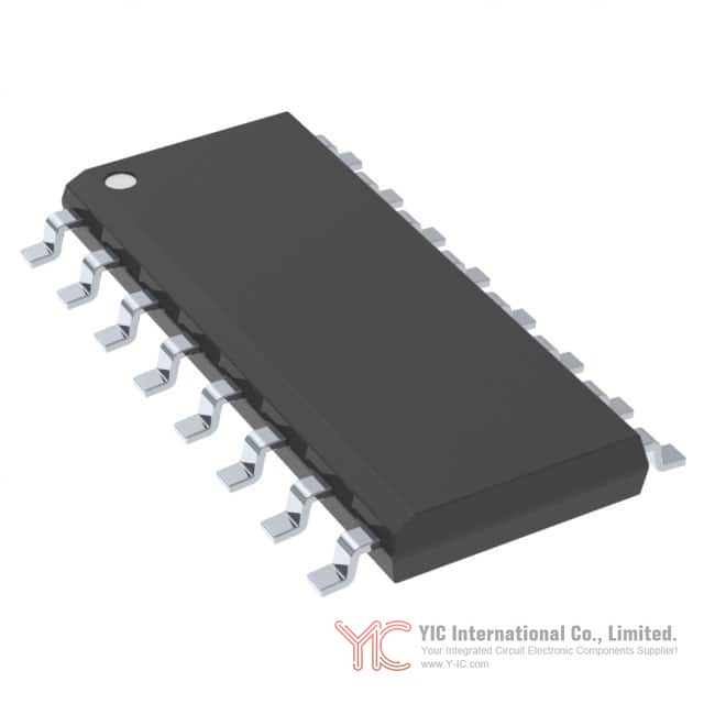
Image may be representation.
See specs for product details.
See specs for product details.
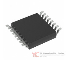
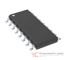
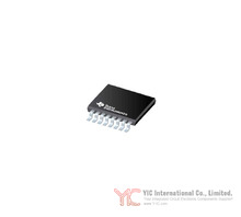
Texas Instruments SN74HCS595DYYR
| Part Number: | SN74HCS595DYYR |
|---|---|
| Manufacturer/Brand: | Texas Instruments |
| Part of Description: | IC LOGIC GATES |
| Datasheets: |
|
| RoHs Status: | Lead free / RoHs compliant |
| Payment: | PayPal / Credit Card / T/T |
| Shipment Way: | DHL / Fedex / TNT / UPS / EMS |
| Share: |
Ship From: Hong Kong
| Quantity | Unit Price |
|---|---|
| 1+ | $0.0629 |
Online RFQ submissions: Fast responses, Better prices!
- Specifications
- Shopping Manual
- Shipping Information
- QC & Packaging
-
Texas Instruments SN74HCS595DYYR technical specifications, attributes, parameters and parts with similar specifications to Texas Instruments SN74HCS595DYYR.Product Attribute Attribute Value Voltage - Supply 2V ~ 6V Supplier Device Package 16-SOT-23-THIN Series 74HCS Package / Case SOT-23-16 Thin, SOT-23 Variant Package Tape & Reel (TR) Output Type Tri-State Operating Temperature -40°C ~ 125°C (TA) Product Attribute Attribute Value Number of Elements 1 Number of Bits per Element 8 Mounting Type Surface Mount Logic Type Shift Register Function Serial to Parallel Base Product Number 74HCS595 -
- Returns Policy
-
Returns must be requested within 60 days of the invoice date and include:
- Original invoice number
- Photo of the parts
- Brief explanation or test report stating the reason for return
Returns will not be accepted after 60 days. Returned items must be in original packaging and resalable condition. Returns due to customer errors at the time of quote or purchase will not be accepted. Contact customer service for return authorization before shipping.
- How to Buy
-
We support both online and offline orders. For detailed guidance on the ordering process, please visit the following link:
https://www.Y-IC.com/RFQ-Quote.htm
If you encounter any issues, feel free to contact our customer service team for assistance.
- Payment
-
We accept the following payment methods:
- T/T in advance (bank transfer)
- Western Union
- Credit Card / Visa / Mastercard / PayPal
Please note that customers are responsible for shipping fees, bank charges, duties, and taxes.

-
- Delivery Period
- Packages will be scheduled for delivery within 1-2 days after all items have arrived at our warehouse. In-stock items will be shipped within 24 hours. The delivery time varies based on the shipping method and the destination.
- Shipping Tracking
- Once the components are delivered, the tracking number will be emailed to you immediately. You can also find the tracking number in your order history.
- Shipping Rate
-
Shipping rates are determined by the size, weight, and destination of the package. YIC provides competitive shipping options through leading carriers such as DHL, FedEx and UPS. Additionally, we offer the option for customers to use their own shipping accounts for direct billing.

-
Quality Control (QC)

Packaging
ESD antistatic protection.
All products are packaged in anti-static bags and shipped with ESD antistatic protection. The label on the external ESD packaging will include our company information: part number, brand, and quantity.
We inspect all goods prior to shipment to ensure they are in excellent condition and verify that the parts are new, original, and match the datasheet specifications. After confirming that everyting is in order,we securely package the items and ship them via global express.


SN74HCS595DYYR Product Details
General Introduction SN74HCS595DYYR 8-bit Serial-In Parallel-Out Register by Texas Instruments
The SN74HCS595DYYR from Texas Instruments is an 8-bit serial-in, parallel-out shift register with 3-state output registers and integrated Schmitt-trigger inputs. Leveraging modern CMOS technology, the device’s architecture makes it a robust and power-efficient solution for expanding digital outputs in a wide range of systems. The SN74HCS595DYYR is part of the SN74HCS595 family, offered in compact SOT-23-THIN packages, as well as other common form factors, supporting design flexibility for dense PCB layouts and scalable output requirements.
Main Attributes and Functional Benefits of SN74HCS595DYYR
At the heart of the SN74HCS595DYYR’s appeal to design engineers are several notable features:
A wide operating voltage range of 2 V to 6 V, allowing compatibility with various logic families.
Schmitt-trigger inputs on all signal pins, enhancing noise immunity and ensuring reliable performance in electrically noisy environments or with slow signal transitions.
High output drive capability, supporting up to ±7.8 mA at 6 V, ideal for driving LEDs or other moderate loads.
Low static power consumption, with a typical quiescent supply current of just 100 nA and typical input leakage currents of ±100 nA.
Separate clocks for shifting and storage, enabling precise timing control over data latching and propagation.
Direct overriding clear input to rapidly reset shift register states.
Cascade capability via serial output, enabling straightforward chaining of multiple devices for large-scale output expansion.
Three-state outputs for flexible bus interfacing and multi-device PCB arrangements.
These attributes position the SN74HCS595DYYR as a versatile and efficient building block for digital output expansion tasks, especially in applications with limited microcontroller or processor I/O resources.
Application Areas and Typical Uses of SN74HCS595DYYR
The SN74HCS595DYYR is well-suited for diverse applications that require an efficient method for digital output expansion. Typical scenarios include LED matrix control, seven-segment display driving, and general-purpose digital output storage. By utilizing the device’s serial-in, parallel-out capability, engineers can reduce microcontroller pin usage from eight or more I/O lines to as few as three or four, with the option to cascade multiple SN74HCS595DYYR units for even wider output expansion requirements. In industrial, consumer, and automotive electronics, this device supports straightforward interfacing and control for indicators, display modules, and more complex peripheral logic.
Pinout Details and Available Package Types for SN74HCS595DYYR
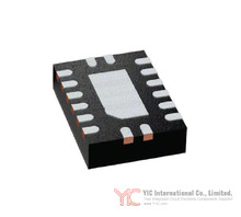
Texas Instruments offers the SN74HCS595DYYR in several package options to support compact and high-density PCB designs. The 16-lead SOT-23-THIN (DYY) package, in particular, addresses space-constrained systems while ensuring thermal and electrical performance. Other available packages include SOIC, TSSOP, and WQFN, each with standard pinouts as detailed in Texas Instruments documentation. The device features pins for serial data input, shift and latch clocks, output enable, clear function, and parallel Q outputs, with dedicated pins to support cascading and output stage control.
Electrical Properties and Timing Parameters of SN74HCS595DYYR
Engineers will find the SN74HCS595DYYR aligns with modern logic requirements. Its performance across temperature ranges of -40°C to +125°C supports industrial-grade reliability. Electrical characteristics include:
Absolute maximum ratings are enforced to protect against overvoltage and overcurrent situations.
ESD immunity is rated for robust manufacturing and handling per JEDEC standards.
Propagation and switching performance is defined for a capacitive load of 50 pF, which is typical for parallel data buses.
The device offers fast switching characteristics suitable for high-speed applications, while Schmitt-trigger inputs guarantee signal clarity, especially in systems with noisy or slow inputs.
Power consumption remains minimal across the full input voltage range, with detailed curves provided for current draw at typical logic levels.
Design and Integration Guidelines for SN74HCS595DYYR
The SN74HCS595DYYR’s balanced CMOS outputs (both 3-state and push-pull) grant flexibility in system design. Engineers should consider drive capability and ensure that output loads (both resistive and capacitive) do not exceed specified device ratings to maintain integrity and avoid thermal damage.
Proper handling of unused inputs and outputs is critical. All unused digital inputs must be tied high or low to ensure device stability, while unused outputs can be left unconnected.
Cascading multiple SN74HCS595DYYR devices requires connecting the serial output of one device to the serial input of the next and synchronizing clock signals, an approach that scales digital expansion efficiently. Initial state indeterminacy on power-up can be managed by clearing the shift registers and initializing outputs as specified.
In display applications, the output enable (OE) pin is especially beneficial, allowing quick disabling of outputs for PWM brightness control or power-down modes without disturbing internal data. The Schmitt-trigger inputs further simplify interfacing with slow-switching buttons or long wiring, reducing spurious switching events.
Power Supply Suggestions and PCB Layout Tips for SN74HCS595DYYR
For optimal operation of the SN74HCS595DYYR, the supply voltage must remain within the 2 V to 6 V range. Each VCC pin should be bypassed with a 0.1-μF capacitor located close to the device, with the option to parallel larger capacitors (like 1 μF) for broad-spectrum noise mitigation. Layout guidelines advocate short trace lengths and minimized capacitive loading (<50 pF) on outputs, along with proper thermal and mechanical consideration for the device’s package.
In multi-channel logic designs, unused inputs must not float; instead, tie them to a defined logic level appropriate for the function.
Mechanical Characteristics and Packaging Details for SN74HCS595DYYR
The SN74HCS595DYYR’s SOT-23-THIN package features a minimal profile and is suited for automated pick-and-place production and reflow soldering. Mechanical and board layout guidelines are available for this and other packages (SOIC, TSSOP, WQFN), as well as recommendations for stencil design and solder paste application. Texas Instruments specifies dimensions and tolerances in conformance with JEDEC and ASME standards, and provides sample board layouts and application notes to minimize assembly risk and ensure reliability.
Alternative and Substitute Devices Comparable to SN74HCS595DYYR
While SN74HCS595DYYR stands out for its power and noise immunity, applications requiring automotive qualification may consider the SN74HCS595-Q1 variant, designed for high-reliability automotive environments. Other similar 8-bit shift registers from Texas Instruments, such as those in the SN74HC595 family, may also serve as replacements, though they may not offer identical Schmitt-trigger input robustness or as wide a voltage operating range.
For alternative vendors, functionally comparable shift registers with serial-in, parallel-out architectures and 3-state outputs may be evaluated, but careful scrutiny of features such as input structure (Schmitt-trigger), ESD ratings, and power consumption is advised to ensure full compatibility.
Conclusion
The SN74HCS595DYYR from Texas Instruments is a highly capable, low-power CMOS shift register designed to facilitate high-density digital output expansion with minimal system resource overhead. Its wide supply voltage range, robust Schmitt-trigger inputs, efficient drive capability, and scalable architecture make it a staple for engineers designing display drivers, output expanders, and general logic interface modules. Adherence to best layout, power, and application guidelines will ensure reliability and performance, while a range of package and equivalent models allows integration into a variety of contemporary electronic systems.
Related Product
SN74HCS595QPWRQ1
G2GHC595A1Z BD2 CORE

SN74HCS594DR
IC SHIFT REGISTER 8 BIT 16SOIC
SN74HCS595QDYYRQ1
AUTOMOTIVE 8-BIT SHIFT REGISTER
SN74HCS594QDRQ1
IC LOGIC GATES
SN74HCS594QBQBRQ1
AUTOMOTIVE 8-BIT SHIFT REGISTERS
SN74HCS595QBQBRQ1
AUTOMOTIVE 8-BIT SHIFT REGISTER
SN74HCS594PWR
IC SHIFT REGISTER 8 BIT 16TSSOP
SN74HCS596QPWRQ1
AUTOMOTIVE 8-BIT SERIAL-IN/PARAL
SN74HCS595PWR
SN74HCS595 CORE
SN74HCS594QWBQBRQ1
AUTOMOTIVE 8-BIT SHIFT REGISTERS
SN74HCS594QDYYRQ1
AUTOMOTIVE 8-BIT SHIFT REGISTERS
SN74HCS595QDRQ1
BD2CORE ISL3 2/28/2020
SN74HCS594DYYR
IC SHIFT REGISTER 8 BIT 16SOT23
SN74HCS595BQBR
8-BIT SHIFT REGISTER WITH SCHMIT
SN74HCS594QPWRQ1
AUTOMOTIVE 8-BIT SHIFT REGISTERS
SN74HCS595QWBQBRQ1
AUTOMOTIVE 8-BIT SHIFT REGISTER
SN74HCS596QDRQ1
AUTOMOTIVE 8-BIT SERIAL-IN/PARAL
SN74HCS595DR
8-BIT SHIFT REGISTER WITH SCHMIT
SN74HCS596PWR
IC SHIFT REGISTER 8 BIT 16TSSOP
SN74HCS596DR
IC SHIFT REGISTER 8 BIT 16SOIC
User Review
-
Powe***b_Engineer
Excellent power MOSFET for high-voltage switching applications. Switching characteristics are predictable and device temperatures stayed within limits.June 15th, 2026
-
Marc***lectronics
This FPGA has been working well in an image processing application. Configuration completed successfully and I have not experienced any reliability issues.June 11th, 2026
-
Sato***Electronics
Reliable DSP controller for motor and signal applications. Performance remained stable and integration with existing hardware was straightforward.June 5th, 2026
-
FPGA***ris
This FPGA worked exactly as expected. Used for signal processing and high-speed data control. Configuration completed without issues and timing closure was easier than expected.May 28th, 2026
-
Robe***lark
Excellent MCU for real-time control and power applications. Stable and fast processing.May 22th, 2026
-
Geor***cott
Works fine as a signal component in timing circuits. No issues so far.May 12th, 2026
-
Oliv***arris
good communicationMay 8th, 2026
-
Bria***lson
Reliable FPGA. Worked smoothly in my MCU + signal integration project.April 28th, 2026
-
Jess***Miller
It works well in my FPGA signal processing setup. Performance is stable and meets the spec without issues so far.April 20th, 2026
-
Powe***sign_Guy
LM5145RGYR works fine in a DC-DC power design. Efficiency is good, but layout needs to be carefully optimized.April 17th, 2026
-
Powe***ive_
Used the FF900R12IP4 in an automotive inverter project. Power handling is solid and thermal performance is stable under load.April 8th, 2026
-
Vipe***rcuit
One unit failed during initial power-up, but the rest were fine. Mixed experience overall.March 31th, 2026
-
Hiro*** T.
Perfect replacement part. My system worked immediately after installation.March 23th, 2026
-
Yuki***
Works very well. I used AD8108ASTZ for video switching project. Stable and no noise problem.March 20th, 2026
-
Jaso***.
Used the AD8108ASTZ in a video routing board and it worked perfectly. Clean switching and no noticeable signal degradation.March 9th, 2026
-
Devo***.
Exactly as described. Great price for a pack of 10.March 4th, 2026
-
Alex***
Moderate quality chip. Works fine at room temperature, but in high temp conditions it seemed to drift. Not terrible, but not premium either.February 28th, 2026
-
Core***nalSourcing
Service was efficient and polite. Components were packed well and labels were clear. Appreciated the attention to detail.February 3th, 2026
-
Nano***icBuyer
Good.January 28th, 2026
-
Quan***Sourcing
Clear communication and quick updates during the whole process. The parts arrived as described. Very satisfied with the service.January 19th, 2026
-
Fusi***oreBuyer
Prompt replies. The order process was smooth and the delivery matched the promised timeline. Satisfied with the service.January 16th, 2026
-
Opti***pSolutions
GoodJanuary 9th, 2026
-
Tech***cuitBuyer
quick answer to our requestDecember 29th, 2025
-
Nova***ponentHub
Recommended, trustedDecember 25th, 2025
-
Grid***ion
Our procurement team relies on YIC for sourcing discontinued parts. They consistently deliver quality and handle cross-references when needed. Great value and support.December 17th, 2025
-
Terr***nse Microtech
Excellent service! We urgently needed a batch of TMS320LF2406APZA for a critical production line. YIC not only offered competitive pricing but also ensured on-time delivery. We’ll definitely reorder.December 10th, 2025
-
Tita***is Industrial
Our urgent production run was saved thanks to their stock of EOL components. Definitely a supplier we will use again.December 4th, 2025
-
Mich***_Embedded
Very professional supplier – confirmed stock quickly and kept me updated until delivery.November 25th, 2025
-
ches***_y
Our EMS line was waiting on MAX3030EEUE+T RS-422 drivers. IC-Components split the shipment—partial now, balance next week—so the SMT schedule didn’t slip. Practical and proactive.November 20th, 2025
-
ca_c***onents_ashley
The goods work as expected and the quote was clear. Only gripe: website showed ‘thousands in stock’ but true on-hand was zero; they turned it around via factory in 5 days and kept me posted. Fair recovery.November 11th, 2025
-
Quin***avis
Needed 250 pcs of LT4256-2IS8#PBF on short notice. They split reels for me, kept the MOQ reasonable, and sent full traceability docs + RoHS/REACH. Will buy again.November 3th, 2025
-
Jaso***ouis
Solid experience end to end. Order arrived faster than expected and the components came in moisture barrier bags with traceable labels.October 30th, 2025
-
AmpC***
The price is good, very satisfied with this purchase.October 22th, 2025
-
Eric***mmons
Great experience overall. The order was processed quickly, and the quality of the electronic components met our expectations.October 16th, 2025
-
Jona***n Brooks
Fast delivery and professional service. Great experience from order to receipt.October 9th, 2025
-
Jess***
Very professional supplier. I received my package quickly, and they were well packed. The team followed up until delivery was complete.September 28th, 2025
-
Sher***
Fast deliverySeptember 17th, 2025
-
Antw***Shawn
I found what I needed, great productSeptember 9th, 2025
-
Shir***neFrame
対応が良くて返信も早いです。発送も早くて助かりました。また買います。September 1th, 2025
-
7ama***
Seller was super nice, product quality is okay, and replies came really fast. Overall, shopping here felt easy and pleasant, would be happy to buy again.August 25th, 2025
-
Zinn***Clarke
Fast shipping, great customer service, and the item came super well-packed. Loved it!August 20th, 2025
-
Josh***Alexander
Outstanding customer support! They’re extremely helpful!July 3th, 2025
-
Lily***nchez
Everything is great!December 18th, 2024
-
Gabr*** Rivera
Great service! Fast shipping! Highly recommended!June 21th, 2023
-
Zoey***ice
The goods were delivered on time and well packaged. Communication with customer service was smooth and easy.April 27th, 2023
-
Madi*** Morgan
We're very satisfied with our purchasing experience at Y-IC, and we're glad to have Jimmy as our point of contact. He responds quickly and always provides competitive pricing.July 1th, 2022
-
Rile***eterson
We had a great experience, with excellent communication and customer support, competitive pricing, and fast delivery.March 4th, 2021
-
Anth*** Butler
I had an excellent experience with Y-IC. Their service was outstanding, and communication was always clear and friendly. All of my questions were answered promptly and professionally. Highly recommended!September 10th, 2020
-
Chlo***ughes
This is the fourth time I've purchased components from here. The quality and service are excellent! My contact is very responsive and highly professional!January 23th, 2020
0 Articles
Sign in to Comment
- Related Categories
- Featured Manufacturers
- Interface - Sensor, Capacitive Touch (642)Specialized ICs (12302)Power Management (PMIC) - Special Purpose Regulators (5644)Power Management (PMIC) - Voltage Regulators - Linear Regulator Controllers (793)Power Management (PMIC) - Voltage Regulators - Linear + Switching (1829)Power Management (PMIC) - Voltage Regulators - Linear, Low Drop Out (LDO) Regulators (70981)Power Management (PMIC) - Voltage Regulators - DC DC Switching Regulators (39569)Power Management (PMIC) - DC DC Switching Controllers (13507)Power Management (PMIC) - Voltage Reference (9453)Power Management (PMIC) - V/F and F/V Converters (145)Power Management (PMIC) - Thermal Management (592)Power Management (PMIC) - Supervisors (47946)


- Blogs & Posts
-
How Fixed Inductors Work in Electronic Circuits
A fixed inductor is designed to provide a stable inductance value that does not change during normal operation. This makes it useful in circuits that ...June 17th, 2026
IR2153 Gate Driver IC Explained: Datasheet, Circuit, and Design Guide
The IR2153 is a high-voltage half-bridge gate driver IC with a built-in oscillator designed for controlling MOSFETs in switching power applications. U...June 17th, 2026
How to Choose the Right Voltage Regulator PMIC for Your Design
Choosing the right voltage regulator PMIC is an important step in designing reliable and efficient electronic systems. A PMIC (Power Management Integr...June 17th, 2026
What is RFID? A Complete Guide to Radio Frequency Identification
RFID helps businesses identify, count, and monitor items without checking each object manually. Although RFID may sound complex, the basic idea is sim...June 16th, 2026
Our Core Strength Our industry certifications & Advantages
SN74HCS595DYYRTexas Instruments |
Quantity*
|
Target Price(USD)
|