


All products are subject to strict incoming inspection and quality control procedures.
We ensure part authenticity, correct specifications, and reliable performance through standardized testing and continuous process improvement.
Quality Warranty
All Categories
-
Integrated Circuits (ICs)
Integrated Circuits (ICs)
- Interface - Sensor, Capacitive Touch(642)
- Specialized ICs(12302)
- Power Management (PMIC) - Special Purpose Regulators(5644)
- Power Management (PMIC) - Voltage Regulators - Linear Regulator Controllers(793)
- Power Management (PMIC) - Voltage Regulators - Linear + Switching(1829)
- Power Management (PMIC) - Voltage Regulators - Linear, Low Drop Out (LDO) Regulators(70981)
- Power Management (PMIC) - Voltage Regulators - DC DC Switching Regulators(39569)
- Power Management (PMIC) - DC DC Switching Controllers(13507)
- Power Management (PMIC) - Voltage Reference(9453)
- Power Management (PMIC) - V/F and F/V Converters(145)
- Power Management (PMIC) - Thermal Management(592)
- Power Management (PMIC) - Supervisors(47946)
- Power Management (PMIC) - RMS to DC Converters(170)
- Power Management (PMIC) - Power Supply Controllers, Monitors(2104)
- Power Management (PMIC) - Power Over Ethernet (PoE) Controllers(1008)
- Power Management (PMIC) - Power Management - Specialized(7722)
- Power Management (PMIC) - Power Distribution Switches, Load Drivers(7706)
- Power Management (PMIC) - PFC (Power Factor Correction)(1222)
- Power Management (PMIC) - OR Controllers, Ideal Diodes(705)
- Power Management (PMIC) - Motor Drivers, Controllers(4712)
- Power Management (PMIC) - Lighting, Ballast Controllers(560)
- Power Management (PMIC) - LED Drivers(7282)
- Power Management (PMIC) - Laser Drivers(573)
- Power Management (PMIC) - Hot Swap Controllers(2816)
- Power Management (PMIC) - Gate Drivers(7083)
- Power Management (PMIC) - Full Half-Bridge (H Bridge) Drivers(1342)
- Power Management (PMIC) - Energy Metering(654)
- Power Management (PMIC) - Display Drivers(1435)
- Power Management (PMIC) - Current Regulation/Management(1481)
- Power Management (PMIC) - Battery Management(5553)
- Power Management (PMIC) - Battery Chargers(3831)
- Power Management (PMIC) - AC DC Converters, Offline Switchers(4905)
- Memory - Controllers(358)
- Memory - Configuration PROMs for FPGAs(639)
- Memory - Batteries(13)
- Memory - Memory(65694)
- Logic - Universal Bus Functions(706)
- Logic - Translators, Level Shifters(2854)
- Logic - Specialty Logic(1870)
- Logic - Signal Switches, Multiplexers, Decoders(9420)
- Logic - Shift Registers(2665)
- Logic - Parity Generators and Checkers(335)
- Logic - Multivibrators(831)
- Logic - Latches(3658)
- Logic - Gates and Inverters - Multi-Function, Configurable(1687)
- Logic - Gates and Inverters(16453)
- Logic - Flip Flops(7780)
- Logic - FIFOs Memory(4240)
- Logic - Counters, Dividers(3456)
- Logic - Comparators(592)
- Logic - Buffers, Drivers, Receivers, Transceivers(17835)
- Linear - Video Processing(2909)
- Linear - Comparators(5084)
- Linear - Analog Multipliers, Dividers(263)
- Linear - Amplifiers - Video Amps and Modules(1905)
- Linear - Amplifiers - Special Purpose(1856)
- Linear - Amplifiers - Instrumentation, OP Amps, Buffer Amps(34236)
- Linear - Amplifiers - Audio(4567)
- Interface - Voice Record and Playback(556)
- Interface - UARTs (Universal Asynchronous Receiver Transmitter)(1237)
- Interface - Telecom(4467)
- Interface - Specialized(4833)
- Interface - Signal Terminators(333)
- Interface - Signal Buffers, Repeaters, Splitters(1449)
- Interface - Serializers, Deserializers(1480)
- Interface - Sensor and Detector Interfaces(1524)
- Interface - Modules(169)
- Interface - Modems - ICs and Modules(407)
- Interface - I/O Expanders(1136)
- Interface - Filters - Active(1226)
- Interface - Encoders, Decoders, Converters(714)
- Interface - Drivers, Receivers, Transceivers(20755)
- Interface - Direct Digital Synthesis (DDS)(117)
- Interface - Controllers(3628)
- Interface - CODECS(1676)
- Interface - Analog Switches, Multiplexers, Demultiplexers(12567)
- Interface - Analog Switches - Special Purpose(2533)
- Embedded - System On Chip (SoC)(4496)
- Embedded - PLDs (Programmable Logic Device)(971)
- Embedded - Microprocessors(10083)
- Embedded - Application Specific Microcontrollers(2275)
- Embedded - Microcontrollers(99285)
- Embedded - Microcontrollers, Microprocessor, FPGA Modules(1527)
- Embedded - FPGAs (Field Programmable Gate Array) with Microcontrollers(81)
- Embedded - FPGAs (Field Programmable Gate Array)(27747)
- Embedded - DSP (Digital Signal Processors)(4081)
- Embedded - CPLDs (Complex Programmable Logic Devices)(5187)
- Data Acquisition - Touch Screen Controllers(1210)
- Data Acquisition - Digital to Analog Converters (DAC)(14419)
- Data Acquisition - Digital Potentiometers(6250)
- Data Acquisition - Analog to Digital Converters (ADC)(17776)
- Data Acquisition - Analog Front End (AFE)(787)
- Data Acquisition - ADCs/DACs - Special Purpose(3043)
- Clock/Timing - Real Time Clocks(2446)
- Clock/Timing - Programmable Timers and Oscillators(23469)
- Clock/Timing - IC Batteries(4)
- Clock/Timing - Delay Lines(1049)
- Clock/Timing - Clock Generators, PLLs, Frequency Synthesizers(32775)
- Clock/Timing - Clock Buffers, Drivers(4568)
- Clock/Timing - Application Specific Clock/Timing(8652)
- Audio Special Purpose(1564)
Relevant Manufacturer


-
Discrete Semiconductor Products
Discrete Semiconductor Products
- Current Regulation - Diodes, Transistors(1090)
- Transistors - Special Purpose(226)
- Transistors - Programmable Unijunction(48)
- Transistors - JFETs(1558)
- Transistors - IGBTs - Single(4799)
- Transistors - IGBTs - Modules(63420)
- Transistors - IGBTs - Arrays(26)
- Transistors - FETs, MOSFETs - Single(48330)
- Transistors - FETs, MOSFETs - RF(4903)
- Transistors - FETs, MOSFETs - Arrays(6641)
- Transistors - Bipolar (BJT) - Single, Pre-Biased(4539)
- Transistors - Bipolar (BJT) - Single(25800)
- Transistors - Bipolar (BJT) - RF(2087)
- Transistors - Bipolar (BJT) - Arrays, Pre-Biased(2115)
- Transistors - Bipolar (BJT) - Arrays(2310)
- Thyristors - TRIACs(4044)
- Thyristors - SCRs - Modules(3967)
- Thyristors - SCRs(5436)
- Thyristors - DIACs, SIDACs(319)
- Power Driver Modules(1627)
- Diodes - Zener - Single(87483)
- Diodes - Zener - Arrays(2619)
- Diodes - Variable Capacitance (Varicaps, Varactors)(1200)
- Diodes - RF Diodes(2753)
- Diodes - Rectifiers - Single(67528)
- Diodes - Rectifiers - Arrays(20581)
- Diodes - Bridge Rectifiers(11700)
Relevant Manufacturer


-
RF and Wireless
RF and Wireless
- Subscriber Identification Module (SIM) Cards(77)
- RF Circulators and Isolators(1742)
- RFID, RF Access, Monitoring ICs(1550)
- RFID Transponders, Tags(747)
- RFID Reader Modules(464)
- RFID Evaluation and Development Kits, Boards(30)
- RFID Antennas(329)
- RFI and EMI - Shielding and Absorbing Materials(6444)
- RFI and EMI - Contacts, Fingerstock and Gaskets(7497)
- RF Transmitters(668)
- RF Transceiver Modules and Modems(6900)
- RF Transceiver ICs(4169)
- RF Switches(9276)
- RF Shields(16401)
- RF Receivers(1998)
- RF Receiver, Transmitter, and Transceiver Finished Units(2763)
- RF Power Dividers/Splitters(1223)
- RF Power Controller ICs(86)
- RF Modulators(710)
- RF Mixers(2800)
- RF Misc ICs and Modules(3276)
- RF Front End (LNA + PA)(419)
- RF Evaluation and Development Kits, Boards(747)
- RF Directional Coupler(2718)
- RF Multiplexers(1464)
- RF Detectors(412)
- RF Demodulators(249)
- RF Antennas(12319)
- RF Amplifiers(19651)
- Balun(1496)
- Attenuators(4852)
Relevant Manufacturer


-
Optoelectronics
Optoelectronics
- Optomechanical(480)
- Lighting Fixtures(125)
- Laser Diodes, Laser Modules - Laser Delivery, Laser Fibers(345)
- HeNe Laser Systems(31)
- HeNe Laser Heads(27)
- Display Backlights(93)
- Xenon Lighting(387)
- Touch Screen Overlays(453)
- Panel Indicators, Pilot Lights(75729)
- Remote Phosphor Light Source(269)
- Reflectors(665)
- Light Pipes(5384)
- Lenses(4951)
- Spacers, Standoffs(2718)
- Lamp Replacements(29718)
- Circuit Board Indicators, Arrays, Light Bars, Bar Graphs(9083)
- LED Thermal Products(667)
- LED Lighting Kits(64)
- LED White Lighting(37580)
- LED Color Lighting(4728)
- LED COBs, Engines, Modules, Strips(28735)
- LED Indication - Discrete(27601)
- Laser Diodes, Modules(1553)
- Incandescent, Neon Lamps(311004)
- Cold Cathode Fluorescent (CCFL) & UV Lamps(164)
- Ballasts, Inverters(7728)
- LED Emitters - Infrared, UV, Visible(3871)
- Fiber Optic Transmitters - Drive Circuitry Integrated(4085)
- Fiber Optic Transmitters - Discrete(350)
- Fiber Optic Transceiver Modules(18758)
- Fiber Optic Switches, Multiplexers, Demultiplexers(1387)
- Fiber Optic Receivers(695)
- Fiber Optic Attenuators(654)
- Electroluminescent(102)
- Display, Monitor - LCD Driver/Controller(98)
- Vacuum Fluorescent (VFD)(249)
- LED Dot Matrix and Cluster(865)
- LED Character and Numeric(5421)
- LCD, OLED, Graphic(4654)
- LCD, OLED Character and Numeric(2202)
- Display Bezels, Lenses(88)
- LED Addressable, Specialty(458)
Relevant Manufacturer


-
Sensors, Transducers
Sensors, Transducers
- Industrial Sensors - Ultrasonic Receivers, Transmitters - Industrial(115)
- Industrial Sensors - Thermostats - Mechanical - Industrial(3103)
- Industrial Sensors - Temperature Sensors - Analog and Digital Output - Industrial(209)
- Industrial Sensors - Proximity Sensors - Industrial(13611)
- Industrial Sensors - Pressure Sensors, Transducers - Industrial(26503)
- Optical Sensors - Photonics - Counters, Detectors, SPCM (Single Photon Counting Module)(751)
- Optical Sensors - Camera Modules(875)
- Industrial Sensors - Position, Proximity, Speed (Modules) - Industrial(554)
- Industrial Sensors - Force Sensors, Load Cells - Industrial(346)
- Industrial Sensors - Flow Sensors - Industrial(151)
- Industrial Sensors - Float, Level Sensors - Industrial(310)
- Industrial Sensors - Encoders - Industrial(4980)
- Industrial Sensors - Color Sensors - Industrial(50)
- Touch Sensors(100)
- Ultrasonic Receivers, Transmitters(2421)
- Temperature Sensors - Thermostats - Solid State(1096)
- Temperature Sensors - Thermostats - Mechanical(3397)
- Temperature Sensors - Thermocouples, Temperature Probes(1921)
- Temperature Sensors - RTD (Resistance Temperature Detector)(1525)
- Temperature Sensors - PTC Thermistors(2273)
- Temperature Sensors - NTC Thermistors(13259)
- Temperature Sensors - Analog and Digital Output(3928)
- Strain Gauges(1399)
- Specialized Sensors(1861)
- Solar Cells(503)
- Shock Sensors(84)
- Sensor Interface - Junction Blocks(2519)
- Sensor Cable - Assemblies(22011)
- Proximity/Occupancy Sensors - Finished Units(725)
- Proximity Sensors(2860)
- Pressure Sensors, Transducers(11317)
- Position Sensors - Angle, Linear Position Measuring(6022)
- Optical Sensors - Reflective - Logic Output(194)
- Optical Sensors - Reflective - Analog Output(432)
- Optical Sensors - Phototransistors(1027)
- Optical Sensors - Photointerrupters - Slot Type - Transistor Output(1427)
- Optical Sensors - Photointerrupters - Slot Type - Logic Output(1215)
- Industrial Sensors - Photoelectric, Industrial(16763)
- Optical Sensors - Photodiodes(1543)
- Optical Sensors - Photo Detectors - Remote Receiver(2605)
- Optical Sensors - Photo Detectors - Logic Output(146)
- Optical Sensors - Photo Detectors - CdS Cells(74)
- Optical Sensors - Distance Measuring(377)
- Optical Sensors - Ambient Light, IR, UV Sensors(1305)
- Multifunction(558)
- Motion Sensors - Vibration Sensors(337)
- Motion Sensors - Tilt Switches(67)
- Motion Sensors - Optical Motion Sensors(719)
- Motion Sensors - Inclinometers(175)
- Motion Sensors - IMUs (Inertial Measurement Units)(416)
- Motion Sensors - Gyroscopes(214)
- Motion Sensors - Accelerometers(1911)
- Magnets - Sensor Matched Magnets(119)
- Magnets - Multi Purpose Magnets(1965)
- Magnetic Sensors - Switches (Solid State)(3700)
- Magnetic Sensors - Position, Proximity, Speed (Modules)(5199)
- Magnetic Sensors - Linear, Compass (ICs)(1247)
- Magnetic Sensors - Compass, Magnetic Field (Modules)(35)
- LVDT Transducers (Linear Variable Differential Transformer)(204)
- IrDA Transceiver Modules(196)
- Optical Sensors - Image Sensors, Camera(2235)
- Humidity, Moisture Sensors(1425)
- Gas Sensors(1217)
- Force Sensors, Load Cells(188)
- Flow Sensors(550)
- Float, Level Sensors(1343)
- Encoders(6357)
- Particle, Dust Sensors(43)
- Current Sensors(3455)
- Color Sensors(85)
- Sensor, Transducer Amplifiers(1905)
Relevant Manufacturer


-
Connectors, Interconnects
Connectors, Interconnects
- USB, DVI, HDMI Connectors(446)
- Solid State Lighting Connectors(555)
- Sockets for ICs, Transistors(953)
- Pluggable Connectors(1221)
- Photovoltaic (Solar Panel) Connectors(136)
- Fiber Optic Connectors(370)
- FFC, FPC (Flat Flexible) Connectors(761)
- D-Sub, D-Shaped Connectors(2887)
- Coaxial Connectors (RF)(2389)
- Circular Connectors(14162)
- Blade Type Power Connectors(273)
- AC Power Connectors - Plugs and Receptacles(2597)
- USB, DVI, HDMI Connectors - USB, DVI, HDMI Connector Adapters(572)
- USB, DVI, HDMI Connectors - USB, DVI, HDMI Connector Assemblies(4298)
- Terminals - Wire to Board Connectors(217)
- Terminals - Wire Splice Connectors(4322)
- Terminals - Wire Pin Connectors(328)
- Terminals - Turret Connectors(1273)
- Terminals - Specialized Connectors(2042)
- Terminals - Spade Connectors(3902)
- Terminals - Solder Lug Connectors(345)
- Terminals - Screw Connectors(745)
- Terminals - Ring Connectors(12596)
- Terminals - Lugs(4747)
- Terminals - Quick Connects, Quick Disconnect Connectors(8514)
- Terminals - PC Pin, Single Post Connectors(3776)
- Terminals - PC Pin Receptacles, Socket Connectors(5883)
- Terminals - Magnetic Wire Connectors(1653)
- Terminals - Knife Connectors(112)
- Terminals - Housings, Boots(2850)
- Terminals - Foil Connectors(108)
- Terminals - Barrel, Bullet Connectors(1107)
- Terminals - Terminal Adapters(137)
- Terminal Strips and Turret Boards(1159)
- Terminal Junction Systems(2533)
- Terminal Blocks - Wire to Board(43615)
- Terminal Blocks - Specialized(3722)
- Terminal Blocks - Power Distribution(847)
- Terminal Blocks - Panel Mount(1359)
- Terminal Blocks - Interface Modules(1819)
- Terminal Blocks - Headers, Plugs and Sockets(119920)
- Terminal Blocks - Din Rail, Channel(9373)
- Terminal Blocks - Terminal Block Contacts(65)
- Terminal Blocks - Barrier Blocks(47517)
- Terminal Blocks - Terminal Block Adapters(1059)
- Solid State Lighting Connectors - Solid State Lighting Connector Contacts(271)
- Solid State Lighting Connectors - Solid State Lighting Connector Assemblies(1344)
- Sockets for ICs, Transistors - Socket Adapters(275)
- Sockets for ICs, Transistors - IC Sockets(22148)
- Shunts, Jumpers(907)
- Rectangular Connectors - Spring Loaded(7721)
- Rectangular Connectors - Rectangular Connector Housings(43023)
- Rectangular Connectors - Headers, Specialty Pin(6129)
- Rectangular Connectors - Headers, Receptacles, Female Sockets(229601)
- Rectangular Connectors - Headers, Male Pins(543338)
- Rectangular Connectors - Free Hanging, Panel Mount(30142)
- Rectangular Connectors - Rectangular Connector Contacts(10681)
- Rectangular Connectors - Board In, Direct Wire to Board(2432)
- Rectangular Connectors - Rectangular Connector Adapters(475)
- Rectangular - Board to Board Connectors - Headers, Receptacles, Female Sockets(9)
- Rectangular - Board to Board Connectors - Headers, Male Pins(2)
- Rectangular Connectors - Board Spacers, Stackers (Board to Board)(238901)
- Rectangular Connectors - Arrays, Edge Type, Mezzanine (Board to Board)(37853)
- AC Power Connectors - Power Entry Modules (PEM)(10310)
- Pluggable Connectors - Pluggable Connector Assemblies(6049)
- Photovoltaic (Solar Panel) Connectors - Photovoltaic (Solar Panel) Connector Contacts(77)
- Photovoltaic (Solar Panel) Connectors - Photovoltaic (Solar Panel) Connector Assemblies(504)
- Modular/Ethernet Connectors - Modular/Ethernet Connector Wiring Blocks(99)
- Modular/Ethernet Connectors - Modular/Ethernet Connector (RJ45, RJ11) Plugs(1674)
- Modular/Ethernet Connectors - Modular/Ethernet Connector Plug Housings(181)
- Modular/Ethernet Connectors - Modular/Ethernet Connector (RJ45) Jacks With Magnetics(10152)
- Modular/Ethernet Connectors - Modular/Ethernet Connector (RJ45, RJ11) Jacks(23416)
- Modular/Ethernet Connectors - Modular/Ethernet Connector Adapters(855)
- Memory Connectors - PC Cards - Adapters(21)
- Memory Connectors - PC Card Sockets(3299)
- Memory Connectors - Inline Module Sockets(3390)
- LGH Connectors(764)
- Keystone Connectors - Keystone Inserts(2758)
- Keystone Connectors - Keystone Faceplates, Frames(1926)
- Heavy Duty Connectors - Heavy Duty Connector Inserts, Modules(4190)
- Heavy Duty Connectors - Heavy Duty Connector Housings, Hoods, Bases(17226)
- Heavy Duty Connectors - Heavy Duty Connector Frames(523)
- Heavy Duty Connectors - Heavy Duty Connector Contacts(1832)
- Heavy Duty Connectors - Heavy Duty Connector Assemblies(671)
- Fiber Optic Connectors - Fiber Optic Connector Housings(919)
- Fiber Optic Connectors - Fiber Optic Connector Adapters(4455)
- Fiber Optic Connectors - Fiber Optic Connector Assemblies(3001)
- FFC, FPC (Flat Flexible) Connectors - FFC, FPC (Flat Flexible) Connector Housings(652)
- FFC, FPC (Flat Flexible) Connectors - FFC, FPC (Flat Flexible) Connector Contacts(202)
- FFC, FPC (Flat Flexible) Connectors - FFC, FPC (Flat Flexible) Connector Assemblies(18691)
- D-Sub, D-Shaped Connectors - D-Sub, D-Shaped Connector Terminators(47)
- D-Sub, D-Shaped Connectors - D-Sub, D-Shaped Connector Housings(12238)
- D-Sub, D-Shaped Connectors - D-Sub, D-Shaped Connector Contacts(2714)
- D-Sub, D-Shaped Connectors - D-Sub, D-Shaped Connector Backshells, Hoods(5995)
- D-Sub, D-Shaped Connectors - D-Sub, D-Shaped Connector Adapters(1304)
- D-Sub, D-Shaped Connectors - D-Sub Connector Assemblies(141346)
- D-Sub, D-Shaped Connectors - Centronics Connectors(8770)
- Contacts - Contacts, Spring Loaded (Pogo Pins), and Pressure(630)
- Contacts - Multi Purpose(6196)
- Contacts - Leadframe(122)
- Coaxial Connectors (RF) - Coaxial Connector (RF) Terminators(1231)
- Coaxial Connectors (RF) - Coaxial Connector (RF) Contacts(480)
- Coaxial Connectors (RF) - Coaxial Connector (RF) Adapters(6386)
- Coaxial Connectors (RF) - Coaxial Connector (RF) Assemblies(25734)
- Circular Connectors - Circular Connector Housings(441226)
- Circular Connectors - Circular Connector Contacts(4737)
- Circular Connectors - Backshells and Cable Clamps(53692)
- Circular Connectors - Circular Connector Adapters(8839)
- Circular Connectors - Circular Connector Assemblies(1196254)
- Card Edge Connectors - Card Edge Connector Housings(469)
- Card Edge Connectors - Edgeboard Connectors(672683)
- Card Edge Connectors - Card Edge Connector Contacts(325)
- Card Edge Connectors - Card Edge Connector Adapters(73)
- Blade Type Power Connectors - Blade Type Power Connector Housings(837)
- Blade Type Power Connectors - Blade Type Power Connector Contacts(393)
- Blade Type Power Connectors - Blade Type Power Connector Assemblies(4163)
- Between Series Adapters(649)
- Barrel Connectors - Power Connectors(935)
- Barrel Connectors - Audio Connectors(2432)
- Barrel Connectors - Barrel Connector Adapters(92)
- Banana and Tip Connectors - Jacks, Plugs(1644)
- Banana and Tip Connectors - Binding Posts(239)
- Banana and Tip Connectors - Banana and Tip Connector Adapters(75)
- Backplane Connectors - Specialized(45586)
- Backplane Connectors - Backplane Connector Housings(6863)
- Backplane Connectors - Hard Metric, Standard(6297)
- Backplane Connectors - DIN 41612(9408)
- Backplane Connectors - Backplane Connector Contacts(3583)
- Backplane Connectors - ARINC Inserts(2357)
- Backplane Connectors - ARINC(3789)
Relevant Manufacturer


-
Resistors
-
Capacitors
Capacitors
- Aluminum Capacitors(16817)
- Trimmers, Variable Capacitors(3151)
- Thin Film Capacitors(3473)
- Tantalum Capacitors(136103)
- Tantalum - Polymer Capacitors(9778)
- Silicon Capacitors(320)
- Niobium Oxide Capacitors(330)
- Mica and PTFE Capacitors(9101)
- Film Capacitors(150406)
- Electric Double Layer Capacitors (EDLC), Supercapacitors(2782)
- Ceramic Capacitors(833829)
- Capacitor Networks, Arrays(2383)
- Aluminum Electrolytic Capacitors(125325)
- Aluminum - Polymer Capacitors(7544)
Relevant Manufacturer


-
Transformers
-
Isolators
Isolators
Relevant Manufacturer


-
Crystals, Oscillators, Resonators
-
Switches
Switches
- Interlock Switches(2893)
- Emergency Stop (E-Stop) Switches(1160)
- Cable Pull Switches(571)
- Toggle Switches(33608)
- Thumbwheel Switches(742)
- Tactile Switches(14263)
- Limit Switches(28077)
- Slide Switches(5166)
- Selector Switches(9720)
- Rotary Switches(13850)
- Rocker Switches(53790)
- Pushbutton Switches - Hall Effect(127)
- Pushbutton Switches(190826)
- Programmable Display Switches(39)
- Navigation Switches, Joystick(1882)
- Magnetic, Reed Switches(1399)
- Keypad Switches(637)
- Keylock Switches(3684)
- DIP Switches(7747)
- Configurable Switch Components - Configurable Switch Lens(1435)
- Configurable Switch Components - Configurable Switch Illumination Sources(1236)
- Configurable Switch Components - Configurable Switch Contact Blocks(1401)
- Configurable Switch Components - Configurable Switch Bodies(16077)
- Disconnect Switch Components(2567)
Relevant Manufacturer


-
Relays
Relays
- Safety Relays(1310)
- Reed Relays(1735)
- High Frequency (RF) Relays(1190)
- Contactors (Solid State)(686)
- Contactors (Electromechanical)(11952)
- Automotive Relays(1881)
- Solid State Relays (SSR)(10652)
- Signal Relays, Up to 2 Amps(9149)
- Relay Sockets(2075)
- Power Relays, Over 2 Amps(31604)
- I/O Relay Modules(712)
- I/O Relay Modules - Input(2)
- I/O Relay Module Racks(247)
Relevant Manufacturer


Select Language
Current Language
English
- English
- Deutsch
- Italia
- Français
- 日本語
- 한국의
- русский
- Svenska
- Nederland
- español
- Português
- polski
- Suomi
- Gaeilge
- Slovenská
- Slovenija
- Čeština
- Melayu
- Magyarország
- Hrvatska
- Dansk
- românesc
- Indonesia
- Ελλάδα
- Български език
- Afrikaans
- IsiXhosa
- isiZulu
- lietuvių
- Maori
- Kongeriket
- Монголулс
- O'zbek
- Tiếng Việt
- हिंदी
- اردو
- Kurdî
- Català
- Bosna
- Euskera
- العربية
- فارسی
- Corsa
- Chicheŵa
- עִבְרִית
- Latviešu
- Hausa
- Беларусь
- አማርኛ
- Republika e Shqipërisë
- Eesti Vabariik
- íslenska
- မြန်မာ
- Македонски
- Lëtzebuergesch
- საქართველო
- Cambodia
- Pilipino
- Azərbaycan
- ພາສາລາວ
- বাংলা ভাষার
- پښتو
- malaɡasʲ
- Кыргыз тили
- Ayiti
- Қазақша
- Samoa
- සිංහල
- ภาษาไทย
- Україна
- Kiswahili
- Cрпски
- Galego
- नेपाली
- Sesotho
- Тоҷикӣ
- Türk dili
- ગુજરાતી
- ಕನ್ನಡkannaḍa
- मराठी

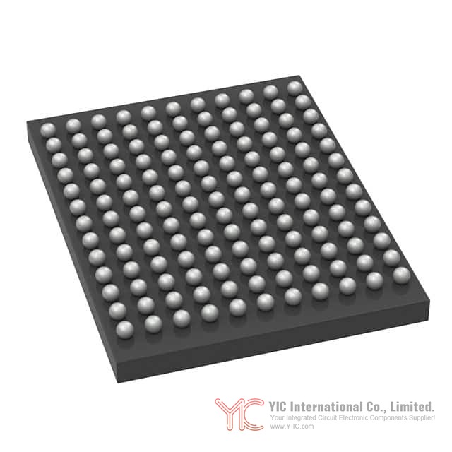
Image may be representation.
See specs for product details.
See specs for product details.
STMicroelectronics STM32F756ZGY6TR
| Part Number: | STM32F756ZGY6TR |
|---|---|
| Manufacturer/Brand: | STMicroelectronics |
| Part of Description: | IC MCU 32BIT 1MB FLASH 143CSP |
| Datasheets: |
|
| RoHs Status: | ROHS3 Compliant |
| Payment: | PayPal / Credit Card / T/T |
| Shipment Way: | DHL / Fedex / TNT / UPS / EMS |
| Share: |
Ship From: Hong Kong
| Quantity | Unit Price |
|---|---|
| 1+ | $24.6036 |
Online RFQ submissions: Fast responses, Better prices!
- Specifications
- Shopping Manual
- Shipping Information
- QC & Packaging
-
STMicroelectronics STM32F756ZGY6TR technical specifications, attributes, parameters and parts with similar specifications to STMicroelectronics STM32F756ZGY6TR.Product Attribute Attribute Value Voltage - Supply (Vcc/Vdd) 1.7V ~ 3.6V Speed 216MHz Series STM32F7 RAM Size 320K x 8 Program Memory Type FLASH Program Memory Size 1MB (1M x 8) Peripherals Brown-out Detect/Reset, DMA, LCD, POR, PWM, WDT Package / Case 143-UFBGA, WLCSP Package Tape & Reel (TR) Oscillator Type Internal Product Attribute Attribute Value Operating Temperature -40°C ~ 85°C (TA) Number of I/O 114 Mounting Type Surface Mount EEPROM Size - Data Converters A/D 24x12b; D/A 2x12b Core Size 32-Bit Single-Core Core Processor ARM® Cortex®-M7 Connectivity CANbus, Ethernet, HDMI-CEC, I²C, IrDA, LINbus, MMC/SD, SAI, SPDIFRX, SPI, UART/USART, USB OTG Base Product Number STM32F756 -
- Returns Policy
-
Returns must be requested within 60 days of the invoice date and include:
- Original invoice number
- Photo of the parts
- Brief explanation or test report stating the reason for return
Returns will not be accepted after 60 days. Returned items must be in original packaging and resalable condition. Returns due to customer errors at the time of quote or purchase will not be accepted. Contact customer service for return authorization before shipping.
- How to Buy
-
We support both online and offline orders. For detailed guidance on the ordering process, please visit the following link:
https://www.Y-IC.com/RFQ-Quote.htm
If you encounter any issues, feel free to contact our customer service team for assistance.
- Payment
-
We accept the following payment methods:
- T/T in advance (bank transfer)
- Western Union
- Credit Card / Visa / Mastercard / PayPal
Please note that customers are responsible for shipping fees, bank charges, duties, and taxes.

-
- Delivery Period
- Packages will be scheduled for delivery within 1-2 days after all items have arrived at our warehouse. In-stock items will be shipped within 24 hours. The delivery time varies based on the shipping method and the destination.
- Shipping Tracking
- Once the components are delivered, the tracking number will be emailed to you immediately. You can also find the tracking number in your order history.
- Shipping Rate
-
Shipping rates are determined by the size, weight, and destination of the package. YIC provides competitive shipping options through leading carriers such as DHL, FedEx and UPS. Additionally, we offer the option for customers to use their own shipping accounts for direct billing.

-
Quality Control (QC)

Packaging
ESD antistatic protection.
All products are packaged in anti-static bags and shipped with ESD antistatic protection. The label on the external ESD packaging will include our company information: part number, brand, and quantity.
We inspect all goods prior to shipment to ensure they are in excellent condition and verify that the parts are new, original, and match the datasheet specifications. After confirming that everyting is in order,we securely package the items and ship them via global express.


STM32F756ZGY6TR Product Details
Product Summary
The STM32F756ZGY6TR from STMicroelectronics is a member of the advanced STM32F7 series of 32-bit microcontrollers designed for high-performance embedded solutions. Based on the ARM Cortex-M7 core, the STM32F756ZGY6TR combines robust processing power (216 MHz operation), significant on-chip memory, and a broad suite of peripherals to address the stringent demands of industrial control, human-machine interfaces, consumer electronics, and communication infrastructure. With its feature-rich specification and scalability, this MCU enables product selection engineers and procurement professionals to deliver maximum capability and design flexibility in their projects.
Main Functions and Performance of the STM32F756ZGY6TR
At the heart of the STM32F756ZGY6TR is an ARM Cortex-M7 CPU, equipped with a floating-point unit (FPU), running at up to 216 MHz. Its high-efficiency core, paired with adaptive real-time accelerator (ART Accelerator™) technology and L1 cache (4 KB each for instructions and data), enables zero-wait state execution when accessing Flash or external memories. This architecture achieves a performance level of up to 462 DMIPS (2.14 DMIPS/MHz, Dhrystone 2.1), backed by extensive DSP instruction support.
This MCU integrates 1 MB of on-chip Flash and a total of 320 KB SRAM, including 64 KB of critical real-time data TCM RAM, 16 KB instruction TCM RAM, and 4 KB of backup SRAM. Its robust performance, memory, and peripheral set are tailored for applications requiring real-time processing, graphic display management, extensive connectivity, and advanced security.
Core Architecture Details of the STM32F756ZGY6TR
The STM32F756ZGY6TR architecture is engineered to support efficient real-time computing and system responsiveness. Key architectural elements include:
Memory protection unit (MPU) for enhanced security and safety.
AXI-AHB multilayer bus matrix for parallel access to critical resources.
Embedded trace macrocell (ETM), SWD, and JTAG interfaces for advanced debugging and trace capabilities.
DMA controller featuring 16 streams with FIFO and burst support, reducing CPU load for data transfers.
Flexible external memory controller (FMC) supporting SRAM, PSRAM, SDRAM, NOR, and NAND memories.
Quad-SPI (QUADSPI) peripheral for high-speed serial memory interfacing.
Engineering teams tasked with applications such as motor control, data acquisition, or HMI display will find the STM32F756ZGY6TR's architecture supports both high-speed algorithm execution and system integration.
Integrated Peripherals and Interface Capabilities of the STM32F756ZGY6TR
The STM32F756ZGY6TR offers extensive on-chip peripheral integration, facilitating advanced system designs:
Up to 25 communication interfaces, featuring multiple USART/UART (ISO 7816, LIN, IrDA), 4x I2C, up to 6x SPI (with I2S for audio class), 2x SAI, CAN (2.0B active), SD/MMC, and Ethernet with IEEE1588 hardware support.
USB 2.0 support (Full-Speed/High-Speed, OTG with on-chip PHY and ULPI), HDMI-CEC, serial audio interfaces, and an 8–14-bit parallel camera interface.
Dedicated LCD-TFT controller with graphics acceleration (Chrom-ART Accelerator™) for up to XGA resolution, making it apt for rich HMIs.
High-precision analog features: three 12-bit, up to 2.4 MSPS ADCs; 2x 12-bit DACs for analog output.
Up to 18 timers (13x 16-bit, 2x 32-bit, watchdogs, PWM, and encoder interfaces) supporting waveform generation and signal timing.
Cryptographic acceleration engine supporting AES128/192/256, Triple DES, SHA, HMAC, and a true random number generator for secure communications.
Such rich peripheral content enables the STM32F756ZGY6TR to serve as the single-chip solution for interconnected, feature-rich embedded devices.
Memory Structure and Data Handling in the STM32F756ZGY6TR
The STM32F756ZGY6TR’s memory organization supports sophisticated data management strategies:
1 MB embedded Flash storage for program code and data.
320 KB SRAM, subdivided to optimize real-time performance (including TCM for ultra-low latency).
OTP (one-time-programmable) memory for storing unique device identifiers or calibration parameters.
Backup SRAM (4 KB) and RTC domain registers retained through VBAT supply for persistent data even during main power loss.
Flexible memory expansion via the FMC for up to 32-bit wide external SRAM, SDRAM, NOR, or NAND Flash.
This well-structured memory system supports deterministic execution, fast context switching, and robust data retention—critical for high-availability and safety-oriented applications.
Energy Management and Low-Power Features of the STM32F756ZGY6TR
Engineered for energy efficiency, the STM32F756ZGY6TR offers several power management features:
Wide supply voltage range (1.7 V to 3.6 V) to support diverse power supply topologies.
Multiple low-power modes (Sleep, Stop, Standby) with fast wake-up times, important for battery-powered or always-on smart devices.
Integrated power-on reset, brown-out reset, programmable voltage detectors, and a dedicated VBAT domain to keep RTC and backup SRAM alive in low-power states.
Dynamic voltage scaling and regulator modes to optimize power based on application state.
These features enable designers to maximize battery life or minimize operational costs without compromising high-speed processing when needed.
Packaging Variants and Pinout for the STM32F756ZGY6TR
The STM32F756ZGY6TR is available in a compact, high-density WLCSP143 (Wafer-Level Chip-Scale Package, 4.5 x 5.8 mm) with 143 I/O pins. STMicroelectronics offers multiple package choices for STM32F7 family members, including LQFP (100, 144, 176, 208 pin), UFBGA, and TFBGA, allowing engineers to select form factors that best fit their PCB and system constraints. The device supports up to 168 I/O ports, of which up to 164 can operate up to 108 MHz. Many I/Os are 5 V-tolerant for compatibility with legacy peripherals, while pin assignments support advanced alternate function mapping for maximal design flexibility.
Electrical Specifications and Thermal Properties of the STM32F756ZGY6TR
The STM32F756ZGY6TR is specified for a broad industrial temperature range (-40°C to +85°C) and is validated for robust operation in adverse environments. It complies with RoHS 3 and is REACH unaffected. Designers benefit from detailed documentation on absolute maximum ratings, power consumption in various modes, oscillator and PLL characteristics, I/O static and AC parameters, EMC, and ESD resilience. The MCU’s thermal characteristics and low power dissipation make it reliable for dense system assemblies.
Alternative or Substitute Models for the STM32F756ZGY6TR
For engineers and procurement professionals exploring alternatives, STMicroelectronics offers multiple pin-to-pin compatible and functionally similar devices within the STM32F7 series. Compatible models include:
STM32F756VG (LQFP100 package)
STM32F756ZG (LQFP144 package)
STM32F756IG (LQFP176 package)
STM32F756BG (UFBGA176 package)
STM32F756NG (LQFP208 package)
Selection can be based on package, available pin count, or specific peripheral subset. Other supplier microcontrollers with ARM Cortex-M7 cores and comparable peripheral integration may be considered; however, differences in memory, I/O mapping, and peripheral features should be carefully reviewed.
Conclusion
The STM32F756ZGY6TR stands as a highly integrated, high-performance MCU, delivering the computational throughput, connectivity, and advanced peripheral integration required for modern embedded designs. Its ARM Cortex-M7 core, rich set of communication and analog peripherals, sophisticated memory system, and robust low-power support position it as a leading candidate for product engineers targeting industrial, consumer, and IoT applications. When selecting an MCU for demanding embedded platforms, the STM32F756ZGY6TR and its family offer a proven balance of flexibility, reliability, and performance.
Related Product

STM32F756IGK6
IC MCU 32BIT 1MB FLASH 176UFBGA
STM32F756NGH6
IC MCU 32BIT 1MB FLASH 216TFBGA
STM32F765IIK6
IC MCU 32BIT 2MB FLASH 176UFBGA
STM32F756ZGY6
STM32F765IGK6
IC MCU 32BIT 1MB FLASH 176UFBGA
STM32F756VGH6
IC MCU 32BIT 1MB FLASH 100TFBGA

STM32F765IIT6
IC MCU 32BIT 2MB FLASH 176LQFP
STM32F765IIK7
IC MCU 32BIT 2MB FLASH 176UFBGA

STM32F756VGT6
IC MCU 32BIT 1MB FLASH 100LQFP
STM32F765BGT6
IC MCU 32BIT 1MB FLASH 208LQFP

STM32F756ZGT6
IC MCU 32BIT 1MB FLASH 144LQFP
STM32F750Z8T6
IC MCU 32BIT 64KB FLASH 144LQFP
STM32F765IGT6
IC MCU 32BIT 1MB FLASH 176LQFP
STM32F756BGT6
IC MCU 32BIT 1MB FLASH 208LQFP
STM32F756IGT6
IC MCU 32BIT 1MB FLASH 176LQFP

STM32F750V8T7
IC MCU 32BIT 64KB FLASH 100LQFP
STM32F765IGK6TR
IC MCU 32BIT 1MB FLASH 176UFBGA
STM32F765BIT6
IC MCU 32BIT 2MB FLASH 208LQFP
STM32F765NGH6
IC MCU 32BIT 1MB FLASH 216TFBGA
STM32F765IIT7
IC MCU 32BIT 2MB FLASH 176LQFP
User Review
-
Geor***cott
Works fine as a signal component in timing circuits. No issues so far.May 12th, 2026
-
Oliv***arris
good communicationMay 8th, 2026
-
Bria***lson
Reliable FPGA. Worked smoothly in my MCU + signal integration project.April 28th, 2026
-
Jess***Miller
It works well in my FPGA signal processing setup. Performance is stable and meets the spec without issues so far.April 20th, 2026
-
Powe***sign_Guy
LM5145RGYR works fine in a DC-DC power design. Efficiency is good, but layout needs to be carefully optimized.April 17th, 2026
-
Powe***ive_
Used the FF900R12IP4 in an automotive inverter project. Power handling is solid and thermal performance is stable under load.April 8th, 2026
-
Vipe***rcuit
One unit failed during initial power-up, but the rest were fine. Mixed experience overall.March 31th, 2026
-
Hiro*** T.
Perfect replacement part. My system worked immediately after installation.March 23th, 2026
-
Yuki***
Works very well. I used AD8108ASTZ for video switching project. Stable and no noise problem.March 20th, 2026
-
Jaso***.
Used the AD8108ASTZ in a video routing board and it worked perfectly. Clean switching and no noticeable signal degradation.March 9th, 2026
-
Devo***.
Exactly as described. Great price for a pack of 10.March 4th, 2026
-
Alex***
Moderate quality chip. Works fine at room temperature, but in high temp conditions it seemed to drift. Not terrible, but not premium either.February 28th, 2026
-
Core***nalSourcing
Service was efficient and polite. Components were packed well and labels were clear. Appreciated the attention to detail.February 3th, 2026
-
Nano***icBuyer
Good.January 28th, 2026
-
Quan***Sourcing
Clear communication and quick updates during the whole process. The parts arrived as described. Very satisfied with the service.January 19th, 2026
-
Fusi***oreBuyer
Prompt replies. The order process was smooth and the delivery matched the promised timeline. Satisfied with the service.January 16th, 2026
-
Opti***pSolutions
GoodJanuary 9th, 2026
-
Tech***cuitBuyer
quick answer to our requestDecember 29th, 2025
-
Nova***ponentHub
Recommended, trustedDecember 25th, 2025
-
Grid***ion
Our procurement team relies on YIC for sourcing discontinued parts. They consistently deliver quality and handle cross-references when needed. Great value and support.December 17th, 2025
-
Terr***nse Microtech
Excellent service! We urgently needed a batch of TMS320LF2406APZA for a critical production line. YIC not only offered competitive pricing but also ensured on-time delivery. We’ll definitely reorder.December 10th, 2025
-
Tita***is Industrial
Our urgent production run was saved thanks to their stock of EOL components. Definitely a supplier we will use again.December 4th, 2025
-
Mich***_Embedded
Very professional supplier – confirmed stock quickly and kept me updated until delivery.November 25th, 2025
-
ches***_y
Our EMS line was waiting on MAX3030EEUE+T RS-422 drivers. IC-Components split the shipment—partial now, balance next week—so the SMT schedule didn’t slip. Practical and proactive.November 20th, 2025
-
ca_c***onents_ashley
The goods work as expected and the quote was clear. Only gripe: website showed ‘thousands in stock’ but true on-hand was zero; they turned it around via factory in 5 days and kept me posted. Fair recovery.November 11th, 2025
-
Quin***avis
Needed 250 pcs of LT4256-2IS8#PBF on short notice. They split reels for me, kept the MOQ reasonable, and sent full traceability docs + RoHS/REACH. Will buy again.November 3th, 2025
-
Jaso***ouis
Solid experience end to end. Order arrived faster than expected and the components came in moisture barrier bags with traceable labels.October 30th, 2025
-
AmpC***
The price is good, very satisfied with this purchase.October 22th, 2025
-
Eric***mmons
Great experience overall. The order was processed quickly, and the quality of the electronic components met our expectations.October 16th, 2025
-
Jona***n Brooks
Fast delivery and professional service. Great experience from order to receipt.October 9th, 2025
-
Jess***
Very professional supplier. I received my package quickly, and they were well packed. The team followed up until delivery was complete.September 28th, 2025
-
Sher***
Fast deliverySeptember 17th, 2025
-
Antw***Shawn
I found what I needed, great productSeptember 9th, 2025
-
Shir***neFrame
対応が良くて返信も早いです。発送も早くて助かりました。また買います。September 1th, 2025
-
7ama***
Seller was super nice, product quality is okay, and replies came really fast. Overall, shopping here felt easy and pleasant, would be happy to buy again.August 25th, 2025
-
Zinn***Clarke
Fast shipping, great customer service, and the item came super well-packed. Loved it!August 20th, 2025
-
Josh***Alexander
Outstanding customer support! They’re extremely helpful!July 3th, 2025
-
Lily***nchez
Everything is great!December 18th, 2024
-
Gabr*** Rivera
Great service! Fast shipping! Highly recommended!June 21th, 2023
-
Zoey***ice
The goods were delivered on time and well packaged. Communication with customer service was smooth and easy.April 27th, 2023
-
Madi*** Morgan
We're very satisfied with our purchasing experience at Y-IC, and we're glad to have Jimmy as our point of contact. He responds quickly and always provides competitive pricing.July 1th, 2022
-
Rile***eterson
We had a great experience, with excellent communication and customer support, competitive pricing, and fast delivery.March 4th, 2021
-
Anth*** Butler
I had an excellent experience with Y-IC. Their service was outstanding, and communication was always clear and friendly. All of my questions were answered promptly and professionally. Highly recommended!September 10th, 2020
-
Chlo***ughes
This is the fourth time I've purchased components from here. The quality and service are excellent! My contact is very responsive and highly professional!January 23th, 2020
0 Articles
Sign in to Comment
- Related Categories
- Featured Manufacturers
- Interface - Sensor, Capacitive Touch (642)Specialized ICs (12302)Power Management (PMIC) - Special Purpose Regulators (5644)Power Management (PMIC) - Voltage Regulators - Linear Regulator Controllers (793)Power Management (PMIC) - Voltage Regulators - Linear + Switching (1829)Power Management (PMIC) - Voltage Regulators - Linear, Low Drop Out (LDO) Regulators (70981)Power Management (PMIC) - Voltage Regulators - DC DC Switching Regulators (39569)Power Management (PMIC) - DC DC Switching Controllers (13507)Power Management (PMIC) - Voltage Reference (9453)Power Management (PMIC) - V/F and F/V Converters (145)Power Management (PMIC) - Thermal Management (592)Power Management (PMIC) - Supervisors (47946)


- Blogs & Posts
-
Lithium-Ion Battery Care Guide for Better Smartphone Battery Life
Smartphone battery life affects how people use their devices every day. Since most smartphones use lithium-ion batteries, understanding how this batte...June 16th, 2026
Inductor Q-Factor Explained: Formula, Effects, and Applications
Inductors are important components in power supplies, filters, RF circuits, and communication systems. However, real inductors are not ideal because t...June 12th, 2026
IR2110 Working Principle and Circuit Design
The IR2110 is a high-voltage MOSFET and IGBT driver IC used to control power switches in demanding electronic circuits. It is designed with separate h...June 12th, 2026
How the INA333 Amplifies Small Sensor Signals
The INA333 instrumentation amplifier IC is designed for accurate measurement of very small differential signals. This article explains the INA333 main...June 12th, 2026
Our Core Strength Our industry certifications & Advantages
 STM32F756ZGY6TRSTMicroelectronics |
Quantity*
|
Target Price(USD)
|