All Categories
-
Integrated Circuits (ICs)
Integrated Circuits (ICs)
- Interface - Sensor, Capacitive Touch(642)
- Specialized ICs(12302)
- Power Management (PMIC) - Special Purpose Regulators(5644)
- Power Management (PMIC) - Voltage Regulators - Linear Regulator Controllers(793)
- Power Management (PMIC) - Voltage Regulators - Linear + Switching(1829)
- Power Management (PMIC) - Voltage Regulators - Linear, Low Drop Out (LDO) Regulators(70981)
- Power Management (PMIC) - Voltage Regulators - DC DC Switching Regulators(39569)
- Power Management (PMIC) - DC DC Switching Controllers(13507)
- Power Management (PMIC) - Voltage Reference(9453)
- Power Management (PMIC) - V/F and F/V Converters(145)
- Power Management (PMIC) - Thermal Management(592)
- Power Management (PMIC) - Supervisors(47946)
- Power Management (PMIC) - RMS to DC Converters(170)
- Power Management (PMIC) - Power Supply Controllers, Monitors(2104)
- Power Management (PMIC) - Power Over Ethernet (PoE) Controllers(1008)
- Power Management (PMIC) - Power Management - Specialized(7722)
- Power Management (PMIC) - Power Distribution Switches, Load Drivers(7706)
- Power Management (PMIC) - PFC (Power Factor Correction)(1222)
- Power Management (PMIC) - OR Controllers, Ideal Diodes(705)
- Power Management (PMIC) - Motor Drivers, Controllers(4712)
- Power Management (PMIC) - Lighting, Ballast Controllers(560)
- Power Management (PMIC) - LED Drivers(7282)
- Power Management (PMIC) - Laser Drivers(573)
- Power Management (PMIC) - Hot Swap Controllers(2816)
- Power Management (PMIC) - Gate Drivers(7083)
- Power Management (PMIC) - Full Half-Bridge (H Bridge) Drivers(1342)
- Power Management (PMIC) - Energy Metering(654)
- Power Management (PMIC) - Display Drivers(1435)
- Power Management (PMIC) - Current Regulation/Management(1481)
- Power Management (PMIC) - Battery Management(5553)
- Power Management (PMIC) - Battery Chargers(3831)
- Power Management (PMIC) - AC DC Converters, Offline Switchers(4905)
- Memory - Controllers(358)
- Memory - Configuration PROMs for FPGAs(639)
- Memory - Batteries(13)
- Memory - Memory(65694)
- Logic - Universal Bus Functions(706)
- Logic - Translators, Level Shifters(2854)
- Logic - Specialty Logic(1870)
- Logic - Signal Switches, Multiplexers, Decoders(9420)
- Logic - Shift Registers(2665)
- Logic - Parity Generators and Checkers(335)
- Logic - Multivibrators(831)
- Logic - Latches(3658)
- Logic - Gates and Inverters - Multi-Function, Configurable(1687)
- Logic - Gates and Inverters(16453)
- Logic - Flip Flops(7780)
- Logic - FIFOs Memory(4240)
- Logic - Counters, Dividers(3456)
- Logic - Comparators(592)
- Logic - Buffers, Drivers, Receivers, Transceivers(17835)
- Linear - Video Processing(2909)
- Linear - Comparators(5084)
- Linear - Analog Multipliers, Dividers(263)
- Linear - Amplifiers - Video Amps and Modules(1905)
- Linear - Amplifiers - Special Purpose(1856)
- Linear - Amplifiers - Instrumentation, OP Amps, Buffer Amps(34236)
- Linear - Amplifiers - Audio(4567)
- Interface - Voice Record and Playback(556)
- Interface - UARTs (Universal Asynchronous Receiver Transmitter)(1237)
- Interface - Telecom(4467)
- Interface - Specialized(4833)
- Interface - Signal Terminators(333)
- Interface - Signal Buffers, Repeaters, Splitters(1449)
- Interface - Serializers, Deserializers(1480)
- Interface - Sensor and Detector Interfaces(1524)
- Interface - Modules(169)
- Interface - Modems - ICs and Modules(407)
- Interface - I/O Expanders(1136)
- Interface - Filters - Active(1226)
- Interface - Encoders, Decoders, Converters(714)
- Interface - Drivers, Receivers, Transceivers(20755)
- Interface - Direct Digital Synthesis (DDS)(117)
- Interface - Controllers(3628)
- Interface - CODECS(1676)
- Interface - Analog Switches, Multiplexers, Demultiplexers(12567)
- Interface - Analog Switches - Special Purpose(2533)
- Embedded - System On Chip (SoC)(4496)
- Embedded - PLDs (Programmable Logic Device)(971)
- Embedded - Microprocessors(10083)
- Embedded - Application Specific Microcontrollers(2275)
- Embedded - Microcontrollers(99285)
- Embedded - Microcontrollers, Microprocessor, FPGA Modules(1527)
- Embedded - FPGAs (Field Programmable Gate Array) with Microcontrollers(81)
- Embedded - FPGAs (Field Programmable Gate Array)(27747)
- Embedded - DSP (Digital Signal Processors)(4081)
- Embedded - CPLDs (Complex Programmable Logic Devices)(5187)
- Data Acquisition - Touch Screen Controllers(1210)
- Data Acquisition - Digital to Analog Converters (DAC)(14419)
- Data Acquisition - Digital Potentiometers(6250)
- Data Acquisition - Analog to Digital Converters (ADC)(17776)
- Data Acquisition - Analog Front End (AFE)(787)
- Data Acquisition - ADCs/DACs - Special Purpose(3043)
- Clock/Timing - Real Time Clocks(2446)
- Clock/Timing - Programmable Timers and Oscillators(23469)
- Clock/Timing - IC Batteries(4)
- Clock/Timing - Delay Lines(1049)
- Clock/Timing - Clock Generators, PLLs, Frequency Synthesizers(32775)
- Clock/Timing - Clock Buffers, Drivers(4568)
- Clock/Timing - Application Specific Clock/Timing(8652)
- Audio Special Purpose(1564)
Relevant Manufacturer


-
Discrete Semiconductor Products
Discrete Semiconductor Products
- Current Regulation - Diodes, Transistors(1090)
- Transistors - Special Purpose(226)
- Transistors - Programmable Unijunction(48)
- Transistors - JFETs(1558)
- Transistors - IGBTs - Single(4799)
- Transistors - IGBTs - Modules(63420)
- Transistors - IGBTs - Arrays(26)
- Transistors - FETs, MOSFETs - Single(48330)
- Transistors - FETs, MOSFETs - RF(4903)
- Transistors - FETs, MOSFETs - Arrays(6641)
- Transistors - Bipolar (BJT) - Single, Pre-Biased(4539)
- Transistors - Bipolar (BJT) - Single(25800)
- Transistors - Bipolar (BJT) - RF(2087)
- Transistors - Bipolar (BJT) - Arrays, Pre-Biased(2115)
- Transistors - Bipolar (BJT) - Arrays(2310)
- Thyristors - TRIACs(4044)
- Thyristors - SCRs - Modules(3967)
- Thyristors - SCRs(5436)
- Thyristors - DIACs, SIDACs(319)
- Power Driver Modules(1627)
- Diodes - Zener - Single(87483)
- Diodes - Zener - Arrays(2619)
- Diodes - Variable Capacitance (Varicaps, Varactors)(1200)
- Diodes - RF Diodes(2753)
- Diodes - Rectifiers - Single(67528)
- Diodes - Rectifiers - Arrays(20581)
- Diodes - Bridge Rectifiers(11700)
Relevant Manufacturer


-
RF and Wireless
RF and Wireless
- Subscriber Identification Module (SIM) Cards(77)
- RF Circulators and Isolators(1742)
- RFID, RF Access, Monitoring ICs(1550)
- RFID Transponders, Tags(747)
- RFID Reader Modules(464)
- RFID Evaluation and Development Kits, Boards(30)
- RFID Antennas(329)
- RFI and EMI - Shielding and Absorbing Materials(6444)
- RFI and EMI - Contacts, Fingerstock and Gaskets(7497)
- RF Transmitters(668)
- RF Transceiver Modules and Modems(6900)
- RF Transceiver ICs(4169)
- RF Switches(9276)
- RF Shields(16401)
- RF Receivers(1998)
- RF Receiver, Transmitter, and Transceiver Finished Units(2763)
- RF Power Dividers/Splitters(1223)
- RF Power Controller ICs(86)
- RF Modulators(710)
- RF Mixers(2800)
- RF Misc ICs and Modules(3276)
- RF Front End (LNA + PA)(419)
- RF Evaluation and Development Kits, Boards(747)
- RF Directional Coupler(2718)
- RF Multiplexers(1464)
- RF Detectors(412)
- RF Demodulators(249)
- RF Antennas(12319)
- RF Amplifiers(19651)
- Balun(1496)
- Attenuators(4852)
Relevant Manufacturer


-
Optoelectronics
Optoelectronics
- Optomechanical(480)
- Lighting Fixtures(125)
- Laser Diodes, Laser Modules - Laser Delivery, Laser Fibers(345)
- HeNe Laser Systems(31)
- HeNe Laser Heads(27)
- Display Backlights(93)
- Xenon Lighting(387)
- Touch Screen Overlays(453)
- Panel Indicators, Pilot Lights(75729)
- Remote Phosphor Light Source(269)
- Reflectors(665)
- Light Pipes(5384)
- Lenses(4951)
- Spacers, Standoffs(2718)
- Lamp Replacements(29718)
- Circuit Board Indicators, Arrays, Light Bars, Bar Graphs(9083)
- LED Thermal Products(667)
- LED Lighting Kits(64)
- LED White Lighting(37580)
- LED Color Lighting(4728)
- LED COBs, Engines, Modules, Strips(28735)
- LED Indication - Discrete(27601)
- Laser Diodes, Modules(1553)
- Incandescent, Neon Lamps(311004)
- Cold Cathode Fluorescent (CCFL) & UV Lamps(164)
- Ballasts, Inverters(7728)
- LED Emitters - Infrared, UV, Visible(3871)
- Fiber Optic Transmitters - Drive Circuitry Integrated(4085)
- Fiber Optic Transmitters - Discrete(350)
- Fiber Optic Transceiver Modules(18758)
- Fiber Optic Switches, Multiplexers, Demultiplexers(1387)
- Fiber Optic Receivers(695)
- Fiber Optic Attenuators(654)
- Electroluminescent(102)
- Display, Monitor - LCD Driver/Controller(98)
- Vacuum Fluorescent (VFD)(249)
- LED Dot Matrix and Cluster(865)
- LED Character and Numeric(5421)
- LCD, OLED, Graphic(4654)
- LCD, OLED Character and Numeric(2202)
- Display Bezels, Lenses(88)
- LED Addressable, Specialty(458)
Relevant Manufacturer


-
Sensors, Transducers
Sensors, Transducers
- Industrial Sensors - Ultrasonic Receivers, Transmitters - Industrial(115)
- Industrial Sensors - Thermostats - Mechanical - Industrial(3103)
- Industrial Sensors - Temperature Sensors - Analog and Digital Output - Industrial(209)
- Industrial Sensors - Proximity Sensors - Industrial(13611)
- Industrial Sensors - Pressure Sensors, Transducers - Industrial(26503)
- Optical Sensors - Photonics - Counters, Detectors, SPCM (Single Photon Counting Module)(751)
- Optical Sensors - Camera Modules(875)
- Industrial Sensors - Position, Proximity, Speed (Modules) - Industrial(554)
- Industrial Sensors - Force Sensors, Load Cells - Industrial(346)
- Industrial Sensors - Flow Sensors - Industrial(151)
- Industrial Sensors - Float, Level Sensors - Industrial(310)
- Industrial Sensors - Encoders - Industrial(4980)
- Industrial Sensors - Color Sensors - Industrial(50)
- Touch Sensors(100)
- Ultrasonic Receivers, Transmitters(2421)
- Temperature Sensors - Thermostats - Solid State(1096)
- Temperature Sensors - Thermostats - Mechanical(3397)
- Temperature Sensors - Thermocouples, Temperature Probes(1921)
- Temperature Sensors - RTD (Resistance Temperature Detector)(1525)
- Temperature Sensors - PTC Thermistors(2273)
- Temperature Sensors - NTC Thermistors(13259)
- Temperature Sensors - Analog and Digital Output(3928)
- Strain Gauges(1399)
- Specialized Sensors(1861)
- Solar Cells(503)
- Shock Sensors(84)
- Sensor Interface - Junction Blocks(2519)
- Sensor Cable - Assemblies(22011)
- Proximity/Occupancy Sensors - Finished Units(725)
- Proximity Sensors(2860)
- Pressure Sensors, Transducers(11317)
- Position Sensors - Angle, Linear Position Measuring(6022)
- Optical Sensors - Reflective - Logic Output(194)
- Optical Sensors - Reflective - Analog Output(432)
- Optical Sensors - Phototransistors(1027)
- Optical Sensors - Photointerrupters - Slot Type - Transistor Output(1427)
- Optical Sensors - Photointerrupters - Slot Type - Logic Output(1215)
- Industrial Sensors - Photoelectric, Industrial(16763)
- Optical Sensors - Photodiodes(1543)
- Optical Sensors - Photo Detectors - Remote Receiver(2605)
- Optical Sensors - Photo Detectors - Logic Output(146)
- Optical Sensors - Photo Detectors - CdS Cells(74)
- Optical Sensors - Distance Measuring(377)
- Optical Sensors - Ambient Light, IR, UV Sensors(1305)
- Multifunction(558)
- Motion Sensors - Vibration Sensors(337)
- Motion Sensors - Tilt Switches(67)
- Motion Sensors - Optical Motion Sensors(719)
- Motion Sensors - Inclinometers(175)
- Motion Sensors - IMUs (Inertial Measurement Units)(416)
- Motion Sensors - Gyroscopes(214)
- Motion Sensors - Accelerometers(1911)
- Magnets - Sensor Matched Magnets(119)
- Magnets - Multi Purpose Magnets(1965)
- Magnetic Sensors - Switches (Solid State)(3700)
- Magnetic Sensors - Position, Proximity, Speed (Modules)(5199)
- Magnetic Sensors - Linear, Compass (ICs)(1247)
- Magnetic Sensors - Compass, Magnetic Field (Modules)(35)
- LVDT Transducers (Linear Variable Differential Transformer)(204)
- IrDA Transceiver Modules(196)
- Optical Sensors - Image Sensors, Camera(2235)
- Humidity, Moisture Sensors(1425)
- Gas Sensors(1217)
- Force Sensors, Load Cells(188)
- Flow Sensors(550)
- Float, Level Sensors(1343)
- Encoders(6357)
- Particle, Dust Sensors(43)
- Current Sensors(3455)
- Color Sensors(85)
- Sensor, Transducer Amplifiers(1905)
Relevant Manufacturer


-
Connectors, Interconnects
Connectors, Interconnects
- USB, DVI, HDMI Connectors(446)
- Solid State Lighting Connectors(555)
- Sockets for ICs, Transistors(953)
- Pluggable Connectors(1221)
- Photovoltaic (Solar Panel) Connectors(136)
- Fiber Optic Connectors(370)
- FFC, FPC (Flat Flexible) Connectors(761)
- D-Sub, D-Shaped Connectors(2887)
- Coaxial Connectors (RF)(2389)
- Circular Connectors(14162)
- Blade Type Power Connectors(273)
- AC Power Connectors - Plugs and Receptacles(2597)
- USB, DVI, HDMI Connectors - USB, DVI, HDMI Connector Adapters(572)
- USB, DVI, HDMI Connectors - USB, DVI, HDMI Connector Assemblies(4298)
- Terminals - Wire to Board Connectors(217)
- Terminals - Wire Splice Connectors(4322)
- Terminals - Wire Pin Connectors(328)
- Terminals - Turret Connectors(1273)
- Terminals - Specialized Connectors(2042)
- Terminals - Spade Connectors(3902)
- Terminals - Solder Lug Connectors(345)
- Terminals - Screw Connectors(745)
- Terminals - Ring Connectors(12596)
- Terminals - Lugs(4747)
- Terminals - Quick Connects, Quick Disconnect Connectors(8514)
- Terminals - PC Pin, Single Post Connectors(3776)
- Terminals - PC Pin Receptacles, Socket Connectors(5883)
- Terminals - Magnetic Wire Connectors(1653)
- Terminals - Knife Connectors(112)
- Terminals - Housings, Boots(2850)
- Terminals - Foil Connectors(108)
- Terminals - Barrel, Bullet Connectors(1107)
- Terminals - Terminal Adapters(137)
- Terminal Strips and Turret Boards(1159)
- Terminal Junction Systems(2533)
- Terminal Blocks - Wire to Board(43615)
- Terminal Blocks - Specialized(3722)
- Terminal Blocks - Power Distribution(847)
- Terminal Blocks - Panel Mount(1359)
- Terminal Blocks - Interface Modules(1819)
- Terminal Blocks - Headers, Plugs and Sockets(119920)
- Terminal Blocks - Din Rail, Channel(9373)
- Terminal Blocks - Terminal Block Contacts(65)
- Terminal Blocks - Barrier Blocks(47517)
- Terminal Blocks - Terminal Block Adapters(1059)
- Solid State Lighting Connectors - Solid State Lighting Connector Contacts(271)
- Solid State Lighting Connectors - Solid State Lighting Connector Assemblies(1344)
- Sockets for ICs, Transistors - Socket Adapters(275)
- Sockets for ICs, Transistors - IC Sockets(22148)
- Shunts, Jumpers(907)
- Rectangular Connectors - Spring Loaded(7721)
- Rectangular Connectors - Rectangular Connector Housings(43023)
- Rectangular Connectors - Headers, Specialty Pin(6129)
- Rectangular Connectors - Headers, Receptacles, Female Sockets(229601)
- Rectangular Connectors - Headers, Male Pins(543338)
- Rectangular Connectors - Free Hanging, Panel Mount(30142)
- Rectangular Connectors - Rectangular Connector Contacts(10681)
- Rectangular Connectors - Board In, Direct Wire to Board(2432)
- Rectangular Connectors - Rectangular Connector Adapters(475)
- Rectangular - Board to Board Connectors - Headers, Receptacles, Female Sockets(9)
- Rectangular - Board to Board Connectors - Headers, Male Pins(2)
- Rectangular Connectors - Board Spacers, Stackers (Board to Board)(238901)
- Rectangular Connectors - Arrays, Edge Type, Mezzanine (Board to Board)(37853)
- AC Power Connectors - Power Entry Modules (PEM)(10310)
- Pluggable Connectors - Pluggable Connector Assemblies(6049)
- Photovoltaic (Solar Panel) Connectors - Photovoltaic (Solar Panel) Connector Contacts(77)
- Photovoltaic (Solar Panel) Connectors - Photovoltaic (Solar Panel) Connector Assemblies(504)
- Modular/Ethernet Connectors - Modular/Ethernet Connector Wiring Blocks(99)
- Modular/Ethernet Connectors - Modular/Ethernet Connector (RJ45, RJ11) Plugs(1674)
- Modular/Ethernet Connectors - Modular/Ethernet Connector Plug Housings(181)
- Modular/Ethernet Connectors - Modular/Ethernet Connector (RJ45) Jacks With Magnetics(10152)
- Modular/Ethernet Connectors - Modular/Ethernet Connector (RJ45, RJ11) Jacks(23416)
- Modular/Ethernet Connectors - Modular/Ethernet Connector Adapters(855)
- Memory Connectors - PC Cards - Adapters(21)
- Memory Connectors - PC Card Sockets(3299)
- Memory Connectors - Inline Module Sockets(3390)
- LGH Connectors(764)
- Keystone Connectors - Keystone Inserts(2758)
- Keystone Connectors - Keystone Faceplates, Frames(1926)
- Heavy Duty Connectors - Heavy Duty Connector Inserts, Modules(4190)
- Heavy Duty Connectors - Heavy Duty Connector Housings, Hoods, Bases(17226)
- Heavy Duty Connectors - Heavy Duty Connector Frames(523)
- Heavy Duty Connectors - Heavy Duty Connector Contacts(1832)
- Heavy Duty Connectors - Heavy Duty Connector Assemblies(671)
- Fiber Optic Connectors - Fiber Optic Connector Housings(919)
- Fiber Optic Connectors - Fiber Optic Connector Adapters(4455)
- Fiber Optic Connectors - Fiber Optic Connector Assemblies(3001)
- FFC, FPC (Flat Flexible) Connectors - FFC, FPC (Flat Flexible) Connector Housings(652)
- FFC, FPC (Flat Flexible) Connectors - FFC, FPC (Flat Flexible) Connector Contacts(202)
- FFC, FPC (Flat Flexible) Connectors - FFC, FPC (Flat Flexible) Connector Assemblies(18691)
- D-Sub, D-Shaped Connectors - D-Sub, D-Shaped Connector Terminators(47)
- D-Sub, D-Shaped Connectors - D-Sub, D-Shaped Connector Housings(12238)
- D-Sub, D-Shaped Connectors - D-Sub, D-Shaped Connector Contacts(2714)
- D-Sub, D-Shaped Connectors - D-Sub, D-Shaped Connector Backshells, Hoods(5995)
- D-Sub, D-Shaped Connectors - D-Sub, D-Shaped Connector Adapters(1304)
- D-Sub, D-Shaped Connectors - D-Sub Connector Assemblies(141346)
- D-Sub, D-Shaped Connectors - Centronics Connectors(8770)
- Contacts - Contacts, Spring Loaded (Pogo Pins), and Pressure(630)
- Contacts - Multi Purpose(6196)
- Contacts - Leadframe(122)
- Coaxial Connectors (RF) - Coaxial Connector (RF) Terminators(1231)
- Coaxial Connectors (RF) - Coaxial Connector (RF) Contacts(480)
- Coaxial Connectors (RF) - Coaxial Connector (RF) Adapters(6386)
- Coaxial Connectors (RF) - Coaxial Connector (RF) Assemblies(25734)
- Circular Connectors - Circular Connector Housings(441226)
- Circular Connectors - Circular Connector Contacts(4737)
- Circular Connectors - Backshells and Cable Clamps(53692)
- Circular Connectors - Circular Connector Adapters(8839)
- Circular Connectors - Circular Connector Assemblies(1196254)
- Card Edge Connectors - Card Edge Connector Housings(469)
- Card Edge Connectors - Edgeboard Connectors(672683)
- Card Edge Connectors - Card Edge Connector Contacts(325)
- Card Edge Connectors - Card Edge Connector Adapters(73)
- Blade Type Power Connectors - Blade Type Power Connector Housings(837)
- Blade Type Power Connectors - Blade Type Power Connector Contacts(393)
- Blade Type Power Connectors - Blade Type Power Connector Assemblies(4163)
- Between Series Adapters(649)
- Barrel Connectors - Power Connectors(935)
- Barrel Connectors - Audio Connectors(2432)
- Barrel Connectors - Barrel Connector Adapters(92)
- Banana and Tip Connectors - Jacks, Plugs(1644)
- Banana and Tip Connectors - Binding Posts(239)
- Banana and Tip Connectors - Banana and Tip Connector Adapters(75)
- Backplane Connectors - Specialized(45586)
- Backplane Connectors - Backplane Connector Housings(6863)
- Backplane Connectors - Hard Metric, Standard(6297)
- Backplane Connectors - DIN 41612(9408)
- Backplane Connectors - Backplane Connector Contacts(3583)
- Backplane Connectors - ARINC Inserts(2357)
- Backplane Connectors - ARINC(3789)
Relevant Manufacturer


-
Resistors
-
Capacitors
Capacitors
- Aluminum Capacitors(16817)
- Trimmers, Variable Capacitors(3151)
- Thin Film Capacitors(3473)
- Tantalum Capacitors(136103)
- Tantalum - Polymer Capacitors(9778)
- Silicon Capacitors(320)
- Niobium Oxide Capacitors(330)
- Mica and PTFE Capacitors(9101)
- Film Capacitors(150406)
- Electric Double Layer Capacitors (EDLC), Supercapacitors(2782)
- Ceramic Capacitors(833829)
- Capacitor Networks, Arrays(2383)
- Aluminum Electrolytic Capacitors(125325)
- Aluminum - Polymer Capacitors(7544)
Relevant Manufacturer


-
Transformers
-
Isolators
Isolators
Relevant Manufacturer


-
Crystals, Oscillators, Resonators
-
Switches
Switches
- Interlock Switches(2893)
- Emergency Stop (E-Stop) Switches(1160)
- Cable Pull Switches(571)
- Toggle Switches(33608)
- Thumbwheel Switches(742)
- Tactile Switches(14263)
- Limit Switches(28077)
- Slide Switches(5166)
- Selector Switches(9720)
- Rotary Switches(13850)
- Rocker Switches(53790)
- Pushbutton Switches - Hall Effect(127)
- Pushbutton Switches(190826)
- Programmable Display Switches(39)
- Navigation Switches, Joystick(1882)
- Magnetic, Reed Switches(1399)
- Keypad Switches(637)
- Keylock Switches(3684)
- DIP Switches(7747)
- Configurable Switch Components - Configurable Switch Lens(1435)
- Configurable Switch Components - Configurable Switch Illumination Sources(1236)
- Configurable Switch Components - Configurable Switch Contact Blocks(1401)
- Configurable Switch Components - Configurable Switch Bodies(16077)
- Disconnect Switch Components(2567)
Relevant Manufacturer


-
Relays
Relays
- Safety Relays(1310)
- Reed Relays(1735)
- High Frequency (RF) Relays(1190)
- Contactors (Solid State)(686)
- Contactors (Electromechanical)(11952)
- Automotive Relays(1881)
- Solid State Relays (SSR)(10652)
- Signal Relays, Up to 2 Amps(9149)
- Relay Sockets(2075)
- Power Relays, Over 2 Amps(31604)
- I/O Relay Modules(712)
- I/O Relay Modules - Input(2)
- I/O Relay Module Racks(247)
Relevant Manufacturer


Select Language
Current Language
English
- English
- Deutsch
- Italia
- Français
- 日本語
- 한국의
- русский
- Svenska
- Nederland
- español
- Português
- polski
- Suomi
- Gaeilge
- Slovenská
- Slovenija
- Čeština
- Melayu
- Magyarország
- Hrvatska
- Dansk
- românesc
- Indonesia
- Ελλάδα
- Български език
- Afrikaans
- IsiXhosa
- isiZulu
- lietuvių
- Maori
- Kongeriket
- Монголулс
- O'zbek
- Tiếng Việt
- हिंदी
- اردو
- Kurdî
- Català
- Bosna
- Euskera
- العربية
- فارسی
- Corsa
- Chicheŵa
- עִבְרִית
- Latviešu
- Hausa
- Беларусь
- አማርኛ
- Republika e Shqipërisë
- Eesti Vabariik
- íslenska
- မြန်မာ
- Македонски
- Lëtzebuergesch
- საქართველო
- Cambodia
- Pilipino
- Azərbaycan
- ພາສາລາວ
- বাংলা ভাষার
- پښتو
- malaɡasʲ
- Кыргыз тили
- Ayiti
- Қазақша
- Samoa
- සිංහල
- ภาษาไทย
- Україна
- Kiswahili
- Cрпски
- Galego
- नेपाली
- Sesotho
- Тоҷикӣ
- Türk dili
- ગુજરાતી
- ಕನ್ನಡkannaḍa
- मराठी
IR2110 Working Principle and Circuit Design
Time: June 12th, 2026
Browse: 5
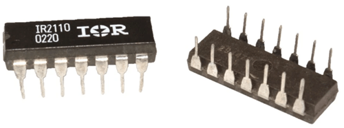
The IR2110 is a high-voltage MOSFET and IGBT driver IC used to control power switches in demanding electronic circuits. It is designed with separate high-side and low-side driver outputs, allowing it to drive two switching devices in circuits such as half-bridge and full-bridge designs. This article will talk about the IR2110's features and specifications, pin configuration, internal architecture, typical application circuits, practical design considerations, comparison with similar driver ICs, selection factors, and popular alternatives.
Catalog
What is IR2110 MOSFET/IGBT Driver IC?
The IR2110 is a high-voltage, high-speed gate driver IC designed to control power MOSFETs and IGBTs. It has independent high-side and low-side output channels, allowing it to drive switching devices with accurate and reliable gate control.
The IR2110 uses rugged CMOS technology, supports standard CMOS and LSTTL logic inputs, and includes a high-pulse-current buffer stage to improve switching performance. Its floating high-side channel can operate up to 500 V, making it suitable for demanding high-voltage circuit designs.
If you are interested in purchasing the IR2110, feel free to contact us for pricing and availability.
Features & Specifications of IR2110
|
Parameter |
Specification |
|
Driver Type |
High-Voltage,
High-Speed MOSFET and IGBT Driver |
|
Number of
Channels |
Independent
High-Side and Low-Side Drivers |
|
Floating Channel
Voltage |
Up to 500 V |
|
Process
Technology |
HVIC and
Latch-Immune CMOS |
|
Logic Input Type |
CMOS and LSTTL
Compatible |
|
Floating Channel
Design |
Designed for
Bootstrap Operation |
|
Gate Drive
Supply Range (VCC) |
10 V to 20 V |
|
VDD Range |
5 V to 20 V |
|
Peak Output
Current (Source) |
2 A Typical |
|
Peak Output
Current (Sink) |
2 A Typical |
|
Undervoltage
Lockout (UVLO) |
Available on
Both Channels |
|
dV/dt Immunity |
High Noise
Immunity |
|
Negative
Transient Voltage |
Tolerant |
|
Input Type |
CMOS Schmitt
Trigger with Pull-Down |
|
Shutdown
Function |
Cycle-by-Cycle
Edge-Triggered Shutdown Logic |
|
Delay Matching |
Matched
Propagation Delay Between Channels |
|
Output
Relationship |
Outputs in Phase
with Inputs |
|
Logic and Power
Ground Offset |
±5 V |
|
High-Speed
Operation |
Optimized for
Fast Switching Applications |
|
Available
Packages |
14-Pin DIP,
16-Pin SOIC |
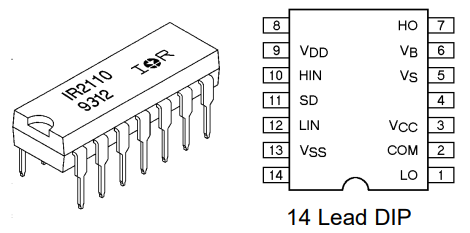
IR2110 Pin Configuration and Pin Functions
|
Pin
No. |
Pin
Name |
Type |
Function |
|
1 |
LO |
Output |
Low-side gate
driver output. Provides the gate drive signal for the low-side MOSFET or
IGBT. |
|
2 |
COM |
Ground |
Low-side return
path and power ground reference for the driver output stage. |
|
3 |
VCC |
Power Supply |
Supply voltage
for the low-side gate driver output stage. Typically 10 V to 20 V. |
|
4 |
NC |
No Connection |
Internal
connection not used. Leave unconnected unless specified by the manufacturer. |
|
5 |
VS |
Floating Return |
Return reference
for the high-side driver. Connected to the source of the high-side MOSFET or
emitter of the high-side IGBT. |
|
6 |
VB |
Floating Supply |
Floating power
supply input for the high-side driver. Usually connected to a bootstrap
capacitor. |
|
7 |
HO |
Output |
High-side gate
driver output. Drives the gate of the high-side MOSFET or IGBT. |
|
8 |
VDD |
Logic Supply |
Logic circuit
supply voltage. Supports logic input stages and internal control circuitry. |
|
9 |
HIN |
Input |
Logic input
controlling the high-side output (HO). A high input turns on the high-side
driver. |
|
10 |
SD |
Input |
Shutdown control
input. Used to disable both driver outputs for fault protection or system
control. |
|
11 |
LIN |
Input |
Logic input
controlling the low-side output (LO). A high input turns on the low-side
driver. |
|
12 |
VSS |
Logic Ground |
Ground reference
for the logic supply and control inputs. |
|
13 |
NC |
No Connection |
Internal
connection not used. Leave unconnected unless specified by the manufacturer. |
|
14 |
NC |
No Connection |
Internal
connection not used. Leave unconnected unless specified by the manufacturer. |
Internal Block Diagram & Architecture of IR2110
The IR2110 contains separate high-side and low-side gate-driver sections designed to control power MOSFETs or IGBTs in switching applications. Inside the device, the input signals pass through Schmitt-trigger circuits that improve noise immunity and ensure reliable operation in electrically noisy environments. Internal logic circuits process the control signals and manage the operation of both driver channels.
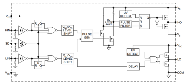
A key part of the architecture is the high-voltage level-shifting circuit. This block transfers control information from the low-voltage logic section to the floating high-side driver section, allowing the device to operate in applications where the switching node moves over a wide voltage range. The floating driver is powered through the VB and VS terminals, enabling proper gate control of the upper switching device.
The IR2110 also incorporates several protection and timing functions. Undervoltage lockout (UVLO) continuously monitors the driver supply voltages and disables the outputs if the voltage falls below a safe operating level. Pulse filtering helps reject unwanted noise pulses, while the shutdown function provides a convenient method for disabling both driver channels during fault conditions or system protection events.
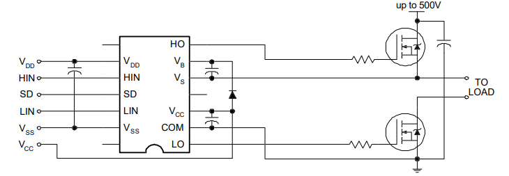
Typical IR2110 Application Circuits
The IR2110 is widely used in half-bridge, full-bridge, and high-power switching circuits. A common application consists of two N-channel MOSFETs connected in a half-bridge arrangement, allowing efficient control of power delivered to a load. This configuration is frequently found in motor drives, DC-AC inverters, switch-mode power supplies, UPS systems, and induction heating equipment.
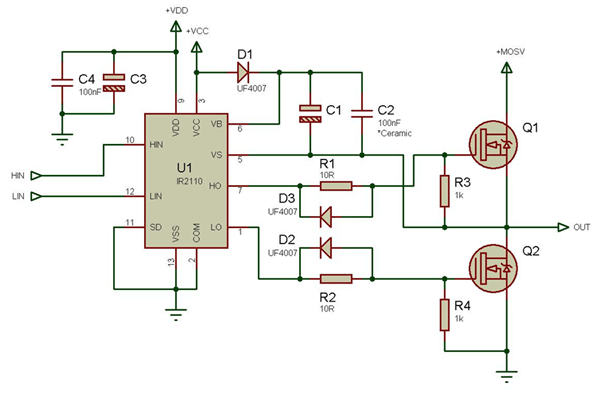
A bootstrap diode and capacitor are typically used to generate the floating supply required by the high-side driver. During operation, the capacitor stores energy and provides the voltage needed to turn on the upper MOSFET. This approach eliminates the need for a separate isolated power source for the high-side gate driver, reducing circuit complexity and cost.
Additional external components are commonly included to improve performance. Gate resistors help control switching speed and reduce voltage ringing, while pull-down resistors ensure the power transistors remain in a defined off-state when no control signal is present. These components contribute to stable and reliable switching operation.
How to Use the IR2110 in Practical Designs
Successful IR2110 designs begin with proper PCB layout and power-supply decoupling. Bypass capacitors should be placed close to the VCC-COM and VDD-VSS pins to reduce voltage dips during fast switching. Gate-drive traces should be short and direct to minimize parasitic inductance, while high-voltage and low-voltage sections should have proper spacing for safety and signal stability.
Gate resistor selection is also important because it controls the MOSFET or IGBT switching speed. A smaller gate resistor gives faster switching but may increase ringing and electromagnetic interference. A larger gate resistor slows the switching edge and can reduce noise, but it may increase switching losses.
The circuit must include proper dead-time control between the high-side and low-side devices. This prevents both switches from turning on at the same time, which can cause shoot-through current and damage the power stage.
For better reliability, you should apply noise reduction techniques such as short ground paths, solid COM connection, proper decoupling, and careful routing of HIN and LIN signals away from noisy switching nodes. Protection recommendations include using undervoltage lockout properly, adding suitable gate resistors, checking bootstrap capacitor size, and protecting the MOSFETs or IGBTs from overcurrent, overvoltage, and overheating.
IR2110 vs IR2101 vs IR2104
|
Feature |
IR2110 |
IR2101 |
IR2104 |
|
Driver Type |
High-Side and
Low-Side Driver |
High-Side and
Low-Side Driver |
High-Side and
Low-Side Driver with Internal Dead Time |
|
High-Side
Floating Supply Voltage |
Up to 500 V |
Up to 600 V |
Up to 600 V |
|
Output Channels |
Independent
High-Side and Low-Side Outputs |
Independent
High-Side and Low-Side Outputs |
Complementary
High-Side and Low-Side Outputs |
|
Peak Output
Current (Source) |
2 A |
130 mA |
210 mA |
|
Peak Output
Current (Sink) |
2 A |
270 mA |
360 mA |
|
Logic Supply
Voltage (VDD) |
5 V to 20 V |
Not Required |
Not Required |
|
Driver Supply
Voltage (VCC) |
10 V to 20 V |
10 V to 20 V |
10 V to 20 V |
|
Logic Input Pins |
HIN, LIN, SD |
HIN, LIN |
IN, SD |
|
Shutdown Pin |
Yes |
No |
Yes |
|
Undervoltage
Lockout (UVLO) |
High-Side and
Low-Side |
High-Side and
Low-Side |
High-Side and
Low-Side |
|
Level Shifter |
Yes |
Yes |
Yes |
|
Bootstrap
Operation |
Yes |
Yes |
Yes |
|
Matched
Propagation Delay |
Yes |
No |
No |
|
Internal Dead
Time |
No |
No |
Yes |
|
Dead-Time
Control |
External |
External |
Internal |
|
Independent
Control of Both Outputs |
Yes |
Yes |
No |
|
Output Logic
Configuration |
Independent |
Independent |
Complementary |
|
Noise Immunity |
High |
High |
High |
|
MOSFET
Compatibility |
N-Channel
MOSFETs |
N-Channel
MOSFETs |
N-Channel
MOSFETs |
|
IGBT
Compatibility |
Yes |
Limited Drive
Capability |
Limited Drive
Capability |
|
Switching
Frequency Capability |
High |
Moderate |
Moderate |
|
Gate Drive
Strength |
High |
Low |
Medium |
|
External
Components Required |
Moderate |
Low |
Low |
|
Design
Complexity |
Moderate |
Simple |
Very Simple |
|
Package Options |
DIP, SOIC |
DIP, SOIC |
DIP, SOIC |
Factors to Consider Before Choosing the IR2110
Switching Frequency Requirements
The IR2110 is designed for high-speed switching and can be used in applications such as inverters, motor drives, and switch-mode power supplies. Before selecting the device, you should evaluate the intended switching frequency and ensure that the MOSFETs or IGBTs can be driven efficiently at that speed. Higher switching frequencies may improve system performance and reduce the size of magnetic components, but they also increase switching losses and heat generation.
MOSFET or IGBT Selection
The IR2110 can drive both N-channel MOSFETs and IGBTs, but the gate-drive requirements of these devices can differ significantly. MOSFETs are generally preferred for high-frequency operation because of their faster switching speed, while IGBTs are often used in higher-voltage and higher-current applications. The selected power device should be compatible with the IR2110's gate-drive voltage and output current capability.
Input Logic Compatibility
The IR2110 supports standard CMOS and LSTTL logic levels, making it compatible with many microcontrollers, DSPs, and PWM controllers. You should verify that the logic output voltage of the control circuit meets the input requirements of the driver to ensure reliable switching and proper signal recognition.
Power Supply Requirements
Proper supply voltages are essential for reliable operation. The IR2110 typically requires a gate-drive supply voltage between 10 V and 20 V, while the high-side driver uses a bootstrap circuit to generate its floating supply. Adequate bypass capacitors and a correctly sized bootstrap capacitor should be included to maintain stable operation during switching.
Isolation Requirements
The IR2110 uses a level-shifting architecture rather than galvanic isolation. For many half-bridge and full-bridge designs, this approach is sufficient and helps reduce circuit complexity. However, applications that require safety isolation, high common-mode noise immunity, or isolated control systems may require an isolated gate driver instead of the IR2110. Evaluating isolation requirements early in the design process helps ensure compliance with system safety and performance requirements.
Popular Alternatives of IR2110
• IR2113
• IRS2110
• IRS2113
• IR2101
• IR2104
• IRS2184
• FAN7392
• UCC27714
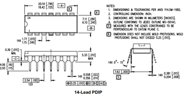
Mechanical Dimensions of IR2110
Conclusion
The IR2110 from Infineon Technologies combines high-side and low-side gate driving, strong output current capability, bootstrap operation, and useful protection features in a single IC. These features help simplify power circuit design while providing reliable control of MOSFETs and IGBTs in high-voltage switching applications. With its independent driver channels, level-shifting architecture, and support for high-speed switching, the IR2110 remains a popular choice for engineers designing inverters, motor drives, power supplies, and other power electronic systems.
Frequently Asked Questions [FAQ]
1. How do you calculate the bootstrap capacitor value for an IR2110 circuit?
The bootstrap capacitor should store enough charge to keep the high-side MOSFET fully enhanced during the entire switching cycle. The value depends on the MOSFET gate charge, switching frequency, leakage currents, and desired voltage margin.
2. Can the IR2110 drive multiple MOSFETs in parallel?
Yes. The IR2110 can drive multiple MOSFETs connected in parallel, provided the total gate charge remains within the driver's capability and proper gate resistors are used for each MOSFET.
3. Why does the high-side MOSFET fail to turn on in some IR2110 designs?
A common cause is an improperly charged bootstrap capacitor. Incorrect bootstrap diode selection, insufficient duty cycle, or wiring errors can also prevent the high-side driver from operating correctly.
4. What happens if no dead time is added between the high-side and low-side switches?
Without sufficient dead time, both switches may conduct simultaneously, causing shoot-through current. This can lead to excessive heating, reduced efficiency, and possible damage to the MOSFETs and driver circuit.
5. Can the IR2110 be used with 3.3 V microcontrollers?
In some cases, yes, but logic-level compatibility should be verified. If the logic signal is not sufficient for reliable operation, a level-shifting circuit may be required.
6. How does gate resistor value affect IR2110 performance?
Smaller gate resistors increase switching speed but may create more ringing and EMI. Larger resistors reduce noise and switching stress but can increase switching losses.
7. What is the maximum practical switching frequency for the IR2110?
The practical limit depends on the MOSFET gate charge, PCB layout, gate resistor values, and power-stage design. Many designs operate successfully from tens of kilohertz to several hundred kilohertz.
8. When should an isolated gate driver be used instead of the IR2110?
An isolated gate driver is often preferred when safety isolation, high common-mode noise immunity, or separate control and power grounds are required by the application.
Related Article
-
![Inductor Q-Factor Explained: Formula, Effects, and Applications]() Jun 12 2026Inductor Q-Factor Explained: Formula, Effects, and Applications
Jun 12 2026Inductor Q-Factor Explained: Formula, Effects, and ApplicationsInductors are important components in power supplies, filters, RF circuits, and communication systems. However, real inductors are not ideal because t... -
![How the INA333 Amplifies Small Sensor Signals]() Jun 12 2026How the INA333 Amplifies Small Sensor Signals
Jun 12 2026How the INA333 Amplifies Small Sensor SignalsThe INA333 instrumentation amplifier IC is designed for accurate measurement of very small differential signals. This article explains the INA333 main...
Related products
GRM033R61E392MA12D
CAP CER 3900PF 25V X5R 0201
GRM0336T1E220GD01D
CAP CER 22PF 25V T2H 0201

TARS156M015
CAP TANT 15UF 20% 15V AXIAL
DMC2400UV-13
MOSFET N/P-CH 20V SOT563

BSP452HUMA1
IC PWR SWTCH N-CHAN 1:1 SOT223-4

PIC18F87K22-I/PT
IC MCU 8BIT 128KB FLASH 80TQFP

MSP430F1132IDW
IC MCU 16BIT 8KB FLASH 20SOIC

MAX4020ESD+T
IC OPAMP VFB 4 CIRCUIT 14SOIC

CD40175BE
IC FF D-TYPE SNGL 4BIT 16DIP
ATM90E32AS-AU-Y
48-TQFP, IND TEMP, 1.8V/3V, TRAY

CX20548-11Z
CX20548-11Z CONEXAN

BD6721FS-GE2
BD6721FS-GE2 ROHM

MC68HC16Z1CFC16
MC68HC16Z1CFC16 FREESCA