


All products are subject to strict incoming inspection and quality control procedures.
We ensure part authenticity, correct specifications, and reliable performance through standardized testing and continuous process improvement.
Quality Warranty
All Categories
-
Integrated Circuits (ICs)
Integrated Circuits (ICs)
- Interface - Sensor, Capacitive Touch(642)
- Specialized ICs(12302)
- Power Management (PMIC) - Special Purpose Regulators(5644)
- Power Management (PMIC) - Voltage Regulators - Linear Regulator Controllers(793)
- Power Management (PMIC) - Voltage Regulators - Linear + Switching(1829)
- Power Management (PMIC) - Voltage Regulators - Linear, Low Drop Out (LDO) Regulators(70981)
- Power Management (PMIC) - Voltage Regulators - DC DC Switching Regulators(39569)
- Power Management (PMIC) - DC DC Switching Controllers(13507)
- Power Management (PMIC) - Voltage Reference(9453)
- Power Management (PMIC) - V/F and F/V Converters(145)
- Power Management (PMIC) - Thermal Management(592)
- Power Management (PMIC) - Supervisors(47946)
- Power Management (PMIC) - RMS to DC Converters(170)
- Power Management (PMIC) - Power Supply Controllers, Monitors(2104)
- Power Management (PMIC) - Power Over Ethernet (PoE) Controllers(1008)
- Power Management (PMIC) - Power Management - Specialized(7722)
- Power Management (PMIC) - Power Distribution Switches, Load Drivers(7706)
- Power Management (PMIC) - PFC (Power Factor Correction)(1222)
- Power Management (PMIC) - OR Controllers, Ideal Diodes(705)
- Power Management (PMIC) - Motor Drivers, Controllers(4712)
- Power Management (PMIC) - Lighting, Ballast Controllers(560)
- Power Management (PMIC) - LED Drivers(7282)
- Power Management (PMIC) - Laser Drivers(573)
- Power Management (PMIC) - Hot Swap Controllers(2816)
- Power Management (PMIC) - Gate Drivers(7083)
- Power Management (PMIC) - Full Half-Bridge (H Bridge) Drivers(1342)
- Power Management (PMIC) - Energy Metering(654)
- Power Management (PMIC) - Display Drivers(1435)
- Power Management (PMIC) - Current Regulation/Management(1481)
- Power Management (PMIC) - Battery Management(5553)
- Power Management (PMIC) - Battery Chargers(3831)
- Power Management (PMIC) - AC DC Converters, Offline Switchers(4905)
- Memory - Controllers(358)
- Memory - Configuration PROMs for FPGAs(639)
- Memory - Batteries(13)
- Memory - Memory(65694)
- Logic - Universal Bus Functions(706)
- Logic - Translators, Level Shifters(2854)
- Logic - Specialty Logic(1870)
- Logic - Signal Switches, Multiplexers, Decoders(9420)
- Logic - Shift Registers(2665)
- Logic - Parity Generators and Checkers(335)
- Logic - Multivibrators(831)
- Logic - Latches(3658)
- Logic - Gates and Inverters - Multi-Function, Configurable(1687)
- Logic - Gates and Inverters(16453)
- Logic - Flip Flops(7780)
- Logic - FIFOs Memory(4240)
- Logic - Counters, Dividers(3456)
- Logic - Comparators(592)
- Logic - Buffers, Drivers, Receivers, Transceivers(17835)
- Linear - Video Processing(2909)
- Linear - Comparators(5084)
- Linear - Analog Multipliers, Dividers(263)
- Linear - Amplifiers - Video Amps and Modules(1905)
- Linear - Amplifiers - Special Purpose(1856)
- Linear - Amplifiers - Instrumentation, OP Amps, Buffer Amps(34236)
- Linear - Amplifiers - Audio(4567)
- Interface - Voice Record and Playback(556)
- Interface - UARTs (Universal Asynchronous Receiver Transmitter)(1237)
- Interface - Telecom(4467)
- Interface - Specialized(4833)
- Interface - Signal Terminators(333)
- Interface - Signal Buffers, Repeaters, Splitters(1449)
- Interface - Serializers, Deserializers(1480)
- Interface - Sensor and Detector Interfaces(1524)
- Interface - Modules(169)
- Interface - Modems - ICs and Modules(407)
- Interface - I/O Expanders(1136)
- Interface - Filters - Active(1226)
- Interface - Encoders, Decoders, Converters(714)
- Interface - Drivers, Receivers, Transceivers(20755)
- Interface - Direct Digital Synthesis (DDS)(117)
- Interface - Controllers(3628)
- Interface - CODECS(1676)
- Interface - Analog Switches, Multiplexers, Demultiplexers(12567)
- Interface - Analog Switches - Special Purpose(2533)
- Embedded - System On Chip (SoC)(4496)
- Embedded - PLDs (Programmable Logic Device)(971)
- Embedded - Microprocessors(10083)
- Embedded - Application Specific Microcontrollers(2275)
- Embedded - Microcontrollers(99285)
- Embedded - Microcontrollers, Microprocessor, FPGA Modules(1527)
- Embedded - FPGAs (Field Programmable Gate Array) with Microcontrollers(81)
- Embedded - FPGAs (Field Programmable Gate Array)(27747)
- Embedded - DSP (Digital Signal Processors)(4081)
- Embedded - CPLDs (Complex Programmable Logic Devices)(5187)
- Data Acquisition - Touch Screen Controllers(1210)
- Data Acquisition - Digital to Analog Converters (DAC)(14419)
- Data Acquisition - Digital Potentiometers(6250)
- Data Acquisition - Analog to Digital Converters (ADC)(17776)
- Data Acquisition - Analog Front End (AFE)(787)
- Data Acquisition - ADCs/DACs - Special Purpose(3043)
- Clock/Timing - Real Time Clocks(2446)
- Clock/Timing - Programmable Timers and Oscillators(23469)
- Clock/Timing - IC Batteries(4)
- Clock/Timing - Delay Lines(1049)
- Clock/Timing - Clock Generators, PLLs, Frequency Synthesizers(32775)
- Clock/Timing - Clock Buffers, Drivers(4568)
- Clock/Timing - Application Specific Clock/Timing(8652)
- Audio Special Purpose(1564)
Relevant Manufacturer


-
Discrete Semiconductor Products
Discrete Semiconductor Products
- Current Regulation - Diodes, Transistors(1090)
- Transistors - Special Purpose(226)
- Transistors - Programmable Unijunction(48)
- Transistors - JFETs(1558)
- Transistors - IGBTs - Single(4799)
- Transistors - IGBTs - Modules(63420)
- Transistors - IGBTs - Arrays(26)
- Transistors - FETs, MOSFETs - Single(48330)
- Transistors - FETs, MOSFETs - RF(4903)
- Transistors - FETs, MOSFETs - Arrays(6641)
- Transistors - Bipolar (BJT) - Single, Pre-Biased(4539)
- Transistors - Bipolar (BJT) - Single(25800)
- Transistors - Bipolar (BJT) - RF(2087)
- Transistors - Bipolar (BJT) - Arrays, Pre-Biased(2115)
- Transistors - Bipolar (BJT) - Arrays(2310)
- Thyristors - TRIACs(4044)
- Thyristors - SCRs - Modules(3967)
- Thyristors - SCRs(5436)
- Thyristors - DIACs, SIDACs(319)
- Power Driver Modules(1627)
- Diodes - Zener - Single(87483)
- Diodes - Zener - Arrays(2619)
- Diodes - Variable Capacitance (Varicaps, Varactors)(1200)
- Diodes - RF Diodes(2753)
- Diodes - Rectifiers - Single(67528)
- Diodes - Rectifiers - Arrays(20581)
- Diodes - Bridge Rectifiers(11700)
Relevant Manufacturer


-
RF and Wireless
RF and Wireless
- Subscriber Identification Module (SIM) Cards(77)
- RF Circulators and Isolators(1742)
- RFID, RF Access, Monitoring ICs(1550)
- RFID Transponders, Tags(747)
- RFID Reader Modules(464)
- RFID Evaluation and Development Kits, Boards(30)
- RFID Antennas(329)
- RFI and EMI - Shielding and Absorbing Materials(6444)
- RFI and EMI - Contacts, Fingerstock and Gaskets(7497)
- RF Transmitters(668)
- RF Transceiver Modules and Modems(6900)
- RF Transceiver ICs(4169)
- RF Switches(9276)
- RF Shields(16401)
- RF Receivers(1998)
- RF Receiver, Transmitter, and Transceiver Finished Units(2763)
- RF Power Dividers/Splitters(1223)
- RF Power Controller ICs(86)
- RF Modulators(710)
- RF Mixers(2800)
- RF Misc ICs and Modules(3276)
- RF Front End (LNA + PA)(419)
- RF Evaluation and Development Kits, Boards(747)
- RF Directional Coupler(2718)
- RF Multiplexers(1464)
- RF Detectors(412)
- RF Demodulators(249)
- RF Antennas(12319)
- RF Amplifiers(19651)
- Balun(1496)
- Attenuators(4852)
Relevant Manufacturer


-
Optoelectronics
Optoelectronics
- Optomechanical(480)
- Lighting Fixtures(125)
- Laser Diodes, Laser Modules - Laser Delivery, Laser Fibers(345)
- HeNe Laser Systems(31)
- HeNe Laser Heads(27)
- Display Backlights(93)
- Xenon Lighting(387)
- Touch Screen Overlays(453)
- Panel Indicators, Pilot Lights(75729)
- Remote Phosphor Light Source(269)
- Reflectors(665)
- Light Pipes(5384)
- Lenses(4951)
- Spacers, Standoffs(2718)
- Lamp Replacements(29718)
- Circuit Board Indicators, Arrays, Light Bars, Bar Graphs(9083)
- LED Thermal Products(667)
- LED Lighting Kits(64)
- LED White Lighting(37580)
- LED Color Lighting(4728)
- LED COBs, Engines, Modules, Strips(28735)
- LED Indication - Discrete(27601)
- Laser Diodes, Modules(1553)
- Incandescent, Neon Lamps(311004)
- Cold Cathode Fluorescent (CCFL) & UV Lamps(164)
- Ballasts, Inverters(7728)
- LED Emitters - Infrared, UV, Visible(3871)
- Fiber Optic Transmitters - Drive Circuitry Integrated(4085)
- Fiber Optic Transmitters - Discrete(350)
- Fiber Optic Transceiver Modules(18758)
- Fiber Optic Switches, Multiplexers, Demultiplexers(1387)
- Fiber Optic Receivers(695)
- Fiber Optic Attenuators(654)
- Electroluminescent(102)
- Display, Monitor - LCD Driver/Controller(98)
- Vacuum Fluorescent (VFD)(249)
- LED Dot Matrix and Cluster(865)
- LED Character and Numeric(5421)
- LCD, OLED, Graphic(4654)
- LCD, OLED Character and Numeric(2202)
- Display Bezels, Lenses(88)
- LED Addressable, Specialty(458)
Relevant Manufacturer


-
Sensors, Transducers
Sensors, Transducers
- Industrial Sensors - Ultrasonic Receivers, Transmitters - Industrial(115)
- Industrial Sensors - Thermostats - Mechanical - Industrial(3103)
- Industrial Sensors - Temperature Sensors - Analog and Digital Output - Industrial(209)
- Industrial Sensors - Proximity Sensors - Industrial(13611)
- Industrial Sensors - Pressure Sensors, Transducers - Industrial(26503)
- Optical Sensors - Photonics - Counters, Detectors, SPCM (Single Photon Counting Module)(751)
- Optical Sensors - Camera Modules(875)
- Industrial Sensors - Position, Proximity, Speed (Modules) - Industrial(554)
- Industrial Sensors - Force Sensors, Load Cells - Industrial(346)
- Industrial Sensors - Flow Sensors - Industrial(151)
- Industrial Sensors - Float, Level Sensors - Industrial(310)
- Industrial Sensors - Encoders - Industrial(4980)
- Industrial Sensors - Color Sensors - Industrial(50)
- Touch Sensors(100)
- Ultrasonic Receivers, Transmitters(2421)
- Temperature Sensors - Thermostats - Solid State(1096)
- Temperature Sensors - Thermostats - Mechanical(3397)
- Temperature Sensors - Thermocouples, Temperature Probes(1921)
- Temperature Sensors - RTD (Resistance Temperature Detector)(1525)
- Temperature Sensors - PTC Thermistors(2273)
- Temperature Sensors - NTC Thermistors(13259)
- Temperature Sensors - Analog and Digital Output(3928)
- Strain Gauges(1399)
- Specialized Sensors(1861)
- Solar Cells(503)
- Shock Sensors(84)
- Sensor Interface - Junction Blocks(2519)
- Sensor Cable - Assemblies(22011)
- Proximity/Occupancy Sensors - Finished Units(725)
- Proximity Sensors(2860)
- Pressure Sensors, Transducers(11317)
- Position Sensors - Angle, Linear Position Measuring(6022)
- Optical Sensors - Reflective - Logic Output(194)
- Optical Sensors - Reflective - Analog Output(432)
- Optical Sensors - Phototransistors(1027)
- Optical Sensors - Photointerrupters - Slot Type - Transistor Output(1427)
- Optical Sensors - Photointerrupters - Slot Type - Logic Output(1215)
- Industrial Sensors - Photoelectric, Industrial(16763)
- Optical Sensors - Photodiodes(1543)
- Optical Sensors - Photo Detectors - Remote Receiver(2605)
- Optical Sensors - Photo Detectors - Logic Output(146)
- Optical Sensors - Photo Detectors - CdS Cells(74)
- Optical Sensors - Distance Measuring(377)
- Optical Sensors - Ambient Light, IR, UV Sensors(1305)
- Multifunction(558)
- Motion Sensors - Vibration Sensors(337)
- Motion Sensors - Tilt Switches(67)
- Motion Sensors - Optical Motion Sensors(719)
- Motion Sensors - Inclinometers(175)
- Motion Sensors - IMUs (Inertial Measurement Units)(416)
- Motion Sensors - Gyroscopes(214)
- Motion Sensors - Accelerometers(1911)
- Magnets - Sensor Matched Magnets(119)
- Magnets - Multi Purpose Magnets(1965)
- Magnetic Sensors - Switches (Solid State)(3700)
- Magnetic Sensors - Position, Proximity, Speed (Modules)(5199)
- Magnetic Sensors - Linear, Compass (ICs)(1247)
- Magnetic Sensors - Compass, Magnetic Field (Modules)(35)
- LVDT Transducers (Linear Variable Differential Transformer)(204)
- IrDA Transceiver Modules(196)
- Optical Sensors - Image Sensors, Camera(2235)
- Humidity, Moisture Sensors(1425)
- Gas Sensors(1217)
- Force Sensors, Load Cells(188)
- Flow Sensors(550)
- Float, Level Sensors(1343)
- Encoders(6357)
- Particle, Dust Sensors(43)
- Current Sensors(3455)
- Color Sensors(85)
- Sensor, Transducer Amplifiers(1905)
Relevant Manufacturer


-
Connectors, Interconnects
Connectors, Interconnects
- USB, DVI, HDMI Connectors(446)
- Solid State Lighting Connectors(555)
- Sockets for ICs, Transistors(953)
- Pluggable Connectors(1221)
- Photovoltaic (Solar Panel) Connectors(136)
- Fiber Optic Connectors(370)
- FFC, FPC (Flat Flexible) Connectors(761)
- D-Sub, D-Shaped Connectors(2887)
- Coaxial Connectors (RF)(2389)
- Circular Connectors(14162)
- Blade Type Power Connectors(273)
- AC Power Connectors - Plugs and Receptacles(2597)
- USB, DVI, HDMI Connectors - USB, DVI, HDMI Connector Adapters(572)
- USB, DVI, HDMI Connectors - USB, DVI, HDMI Connector Assemblies(4298)
- Terminals - Wire to Board Connectors(217)
- Terminals - Wire Splice Connectors(4322)
- Terminals - Wire Pin Connectors(328)
- Terminals - Turret Connectors(1273)
- Terminals - Specialized Connectors(2042)
- Terminals - Spade Connectors(3902)
- Terminals - Solder Lug Connectors(345)
- Terminals - Screw Connectors(745)
- Terminals - Ring Connectors(12596)
- Terminals - Lugs(4747)
- Terminals - Quick Connects, Quick Disconnect Connectors(8514)
- Terminals - PC Pin, Single Post Connectors(3776)
- Terminals - PC Pin Receptacles, Socket Connectors(5883)
- Terminals - Magnetic Wire Connectors(1653)
- Terminals - Knife Connectors(112)
- Terminals - Housings, Boots(2850)
- Terminals - Foil Connectors(108)
- Terminals - Barrel, Bullet Connectors(1107)
- Terminals - Terminal Adapters(137)
- Terminal Strips and Turret Boards(1159)
- Terminal Junction Systems(2533)
- Terminal Blocks - Wire to Board(43615)
- Terminal Blocks - Specialized(3722)
- Terminal Blocks - Power Distribution(847)
- Terminal Blocks - Panel Mount(1359)
- Terminal Blocks - Interface Modules(1819)
- Terminal Blocks - Headers, Plugs and Sockets(119920)
- Terminal Blocks - Din Rail, Channel(9373)
- Terminal Blocks - Terminal Block Contacts(65)
- Terminal Blocks - Barrier Blocks(47517)
- Terminal Blocks - Terminal Block Adapters(1059)
- Solid State Lighting Connectors - Solid State Lighting Connector Contacts(271)
- Solid State Lighting Connectors - Solid State Lighting Connector Assemblies(1344)
- Sockets for ICs, Transistors - Socket Adapters(275)
- Sockets for ICs, Transistors - IC Sockets(22148)
- Shunts, Jumpers(907)
- Rectangular Connectors - Spring Loaded(7721)
- Rectangular Connectors - Rectangular Connector Housings(43023)
- Rectangular Connectors - Headers, Specialty Pin(6129)
- Rectangular Connectors - Headers, Receptacles, Female Sockets(229601)
- Rectangular Connectors - Headers, Male Pins(543338)
- Rectangular Connectors - Free Hanging, Panel Mount(30142)
- Rectangular Connectors - Rectangular Connector Contacts(10681)
- Rectangular Connectors - Board In, Direct Wire to Board(2432)
- Rectangular Connectors - Rectangular Connector Adapters(475)
- Rectangular - Board to Board Connectors - Headers, Receptacles, Female Sockets(9)
- Rectangular - Board to Board Connectors - Headers, Male Pins(2)
- Rectangular Connectors - Board Spacers, Stackers (Board to Board)(238901)
- Rectangular Connectors - Arrays, Edge Type, Mezzanine (Board to Board)(37853)
- AC Power Connectors - Power Entry Modules (PEM)(10310)
- Pluggable Connectors - Pluggable Connector Assemblies(6049)
- Photovoltaic (Solar Panel) Connectors - Photovoltaic (Solar Panel) Connector Contacts(77)
- Photovoltaic (Solar Panel) Connectors - Photovoltaic (Solar Panel) Connector Assemblies(504)
- Modular/Ethernet Connectors - Modular/Ethernet Connector Wiring Blocks(99)
- Modular/Ethernet Connectors - Modular/Ethernet Connector (RJ45, RJ11) Plugs(1674)
- Modular/Ethernet Connectors - Modular/Ethernet Connector Plug Housings(181)
- Modular/Ethernet Connectors - Modular/Ethernet Connector (RJ45) Jacks With Magnetics(10152)
- Modular/Ethernet Connectors - Modular/Ethernet Connector (RJ45, RJ11) Jacks(23416)
- Modular/Ethernet Connectors - Modular/Ethernet Connector Adapters(855)
- Memory Connectors - PC Cards - Adapters(21)
- Memory Connectors - PC Card Sockets(3299)
- Memory Connectors - Inline Module Sockets(3390)
- LGH Connectors(764)
- Keystone Connectors - Keystone Inserts(2758)
- Keystone Connectors - Keystone Faceplates, Frames(1926)
- Heavy Duty Connectors - Heavy Duty Connector Inserts, Modules(4190)
- Heavy Duty Connectors - Heavy Duty Connector Housings, Hoods, Bases(17226)
- Heavy Duty Connectors - Heavy Duty Connector Frames(523)
- Heavy Duty Connectors - Heavy Duty Connector Contacts(1832)
- Heavy Duty Connectors - Heavy Duty Connector Assemblies(671)
- Fiber Optic Connectors - Fiber Optic Connector Housings(919)
- Fiber Optic Connectors - Fiber Optic Connector Adapters(4455)
- Fiber Optic Connectors - Fiber Optic Connector Assemblies(3001)
- FFC, FPC (Flat Flexible) Connectors - FFC, FPC (Flat Flexible) Connector Housings(652)
- FFC, FPC (Flat Flexible) Connectors - FFC, FPC (Flat Flexible) Connector Contacts(202)
- FFC, FPC (Flat Flexible) Connectors - FFC, FPC (Flat Flexible) Connector Assemblies(18691)
- D-Sub, D-Shaped Connectors - D-Sub, D-Shaped Connector Terminators(47)
- D-Sub, D-Shaped Connectors - D-Sub, D-Shaped Connector Housings(12238)
- D-Sub, D-Shaped Connectors - D-Sub, D-Shaped Connector Contacts(2714)
- D-Sub, D-Shaped Connectors - D-Sub, D-Shaped Connector Backshells, Hoods(5995)
- D-Sub, D-Shaped Connectors - D-Sub, D-Shaped Connector Adapters(1304)
- D-Sub, D-Shaped Connectors - D-Sub Connector Assemblies(141346)
- D-Sub, D-Shaped Connectors - Centronics Connectors(8770)
- Contacts - Contacts, Spring Loaded (Pogo Pins), and Pressure(630)
- Contacts - Multi Purpose(6196)
- Contacts - Leadframe(122)
- Coaxial Connectors (RF) - Coaxial Connector (RF) Terminators(1231)
- Coaxial Connectors (RF) - Coaxial Connector (RF) Contacts(480)
- Coaxial Connectors (RF) - Coaxial Connector (RF) Adapters(6386)
- Coaxial Connectors (RF) - Coaxial Connector (RF) Assemblies(25734)
- Circular Connectors - Circular Connector Housings(441226)
- Circular Connectors - Circular Connector Contacts(4737)
- Circular Connectors - Backshells and Cable Clamps(53692)
- Circular Connectors - Circular Connector Adapters(8839)
- Circular Connectors - Circular Connector Assemblies(1196254)
- Card Edge Connectors - Card Edge Connector Housings(469)
- Card Edge Connectors - Edgeboard Connectors(672683)
- Card Edge Connectors - Card Edge Connector Contacts(325)
- Card Edge Connectors - Card Edge Connector Adapters(73)
- Blade Type Power Connectors - Blade Type Power Connector Housings(837)
- Blade Type Power Connectors - Blade Type Power Connector Contacts(393)
- Blade Type Power Connectors - Blade Type Power Connector Assemblies(4163)
- Between Series Adapters(649)
- Barrel Connectors - Power Connectors(935)
- Barrel Connectors - Audio Connectors(2432)
- Barrel Connectors - Barrel Connector Adapters(92)
- Banana and Tip Connectors - Jacks, Plugs(1644)
- Banana and Tip Connectors - Binding Posts(239)
- Banana and Tip Connectors - Banana and Tip Connector Adapters(75)
- Backplane Connectors - Specialized(45586)
- Backplane Connectors - Backplane Connector Housings(6863)
- Backplane Connectors - Hard Metric, Standard(6297)
- Backplane Connectors - DIN 41612(9408)
- Backplane Connectors - Backplane Connector Contacts(3583)
- Backplane Connectors - ARINC Inserts(2357)
- Backplane Connectors - ARINC(3789)
Relevant Manufacturer


-
Resistors
-
Capacitors
Capacitors
- Aluminum Capacitors(16817)
- Trimmers, Variable Capacitors(3151)
- Thin Film Capacitors(3473)
- Tantalum Capacitors(136103)
- Tantalum - Polymer Capacitors(9778)
- Silicon Capacitors(320)
- Niobium Oxide Capacitors(330)
- Mica and PTFE Capacitors(9101)
- Film Capacitors(150406)
- Electric Double Layer Capacitors (EDLC), Supercapacitors(2782)
- Ceramic Capacitors(833829)
- Capacitor Networks, Arrays(2383)
- Aluminum Electrolytic Capacitors(125325)
- Aluminum - Polymer Capacitors(7544)
Relevant Manufacturer


-
Transformers
-
Isolators
Isolators
Relevant Manufacturer


-
Crystals, Oscillators, Resonators
-
Switches
Switches
- Interlock Switches(2893)
- Emergency Stop (E-Stop) Switches(1160)
- Cable Pull Switches(571)
- Toggle Switches(33608)
- Thumbwheel Switches(742)
- Tactile Switches(14263)
- Limit Switches(28077)
- Slide Switches(5166)
- Selector Switches(9720)
- Rotary Switches(13850)
- Rocker Switches(53790)
- Pushbutton Switches - Hall Effect(127)
- Pushbutton Switches(190826)
- Programmable Display Switches(39)
- Navigation Switches, Joystick(1882)
- Magnetic, Reed Switches(1399)
- Keypad Switches(637)
- Keylock Switches(3684)
- DIP Switches(7747)
- Configurable Switch Components - Configurable Switch Lens(1435)
- Configurable Switch Components - Configurable Switch Illumination Sources(1236)
- Configurable Switch Components - Configurable Switch Contact Blocks(1401)
- Configurable Switch Components - Configurable Switch Bodies(16077)
- Disconnect Switch Components(2567)
Relevant Manufacturer


-
Relays
Relays
- Safety Relays(1310)
- Reed Relays(1735)
- High Frequency (RF) Relays(1190)
- Contactors (Solid State)(686)
- Contactors (Electromechanical)(11952)
- Automotive Relays(1881)
- Solid State Relays (SSR)(10652)
- Signal Relays, Up to 2 Amps(9149)
- Relay Sockets(2075)
- Power Relays, Over 2 Amps(31604)
- I/O Relay Modules(712)
- I/O Relay Modules - Input(2)
- I/O Relay Module Racks(247)
Relevant Manufacturer


Select Language
Current Language
English
- English
- Deutsch
- Italia
- Français
- 日本語
- 한국의
- русский
- Svenska
- Nederland
- español
- Português
- polski
- Suomi
- Gaeilge
- Slovenská
- Slovenija
- Čeština
- Melayu
- Magyarország
- Hrvatska
- Dansk
- românesc
- Indonesia
- Ελλάδα
- Български език
- Afrikaans
- IsiXhosa
- isiZulu
- lietuvių
- Maori
- Kongeriket
- Монголулс
- O'zbek
- Tiếng Việt
- हिंदी
- اردو
- Kurdî
- Català
- Bosna
- Euskera
- العربية
- فارسی
- Corsa
- Chicheŵa
- עִבְרִית
- Latviešu
- Hausa
- Беларусь
- አማርኛ
- Republika e Shqipërisë
- Eesti Vabariik
- íslenska
- မြန်မာ
- Македонски
- Lëtzebuergesch
- საქართველო
- Cambodia
- Pilipino
- Azərbaycan
- ພາສາລາວ
- বাংলা ভাষার
- پښتو
- malaɡasʲ
- Кыргыз тили
- Ayiti
- Қазақша
- Samoa
- සිංහල
- ภาษาไทย
- Україна
- Kiswahili
- Cрпски
- Galego
- नेपाली
- Sesotho
- Тоҷикӣ
- Türk dili
- ગુજરાતી
- ಕನ್ನಡkannaḍa
- मराठी
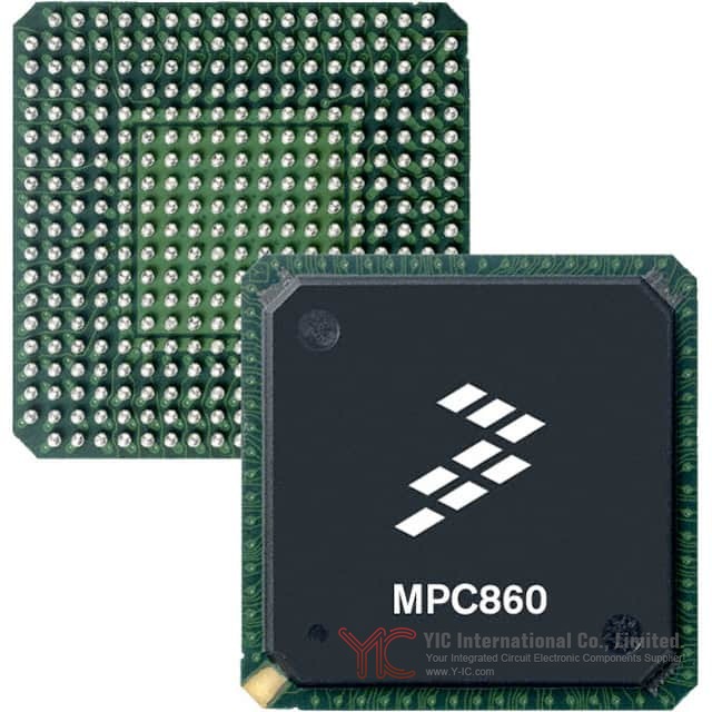
Image may be representation.
See specs for product details.
See specs for product details.
NXP USA Inc. MPC855TCVR50D4R2
| Part Number: | MPC855TCVR50D4R2 |
|---|---|
| Manufacturer/Brand: | NXP USA Inc. |
| Part of Description: | IC MPU MPC8XX 50MHZ 357BGA |
| Datasheets: |
|
| RoHs Status: | ROHS3 Compliant |
| Payment: | PayPal / Credit Card / T/T |
| Shipment Way: | DHL / Fedex / TNT / UPS / EMS |
| Share: |
Ship From: Hong Kong
Get the lowest prices by enquiry
Online RFQ submissions: Fast responses, Better prices!
- Specifications
- Shopping Manual
- Shipping Information
- QC & Packaging
-
NXP USA Inc. MPC855TCVR50D4R2 technical specifications, attributes, parameters and parts with similar specifications to NXP USA Inc. MPC855TCVR50D4R2.Product Attribute Attribute Value Voltage - I/O 3.3V USB - Supplier Device Package 357-PBGA (25x25) Speed 50MHz Series MPC8xx Security Features - SATA - RAM Controllers DRAM Package / Case 357-BBGA Package Tape & Reel (TR) Product Attribute Attribute Value Operating Temperature -40°C ~ 95°C (TA) Number of Cores/Bus Width 1 Core, 32-Bit Mounting Type Surface Mount Graphics Acceleration No Ethernet 10Mbps (1), 10/100Mbps (1) Display & Interface Controllers - Core Processor MPC8xx Co-Processors/DSP Communications; CPM Base Product Number MPC85 Additional Interfaces HDLC/SDLC, I²C, IrDA, PCMCIA, SPI, TDM, UART/USART -
- Returns Policy
-
Returns must be requested within 60 days of the invoice date and include:
- Original invoice number
- Photo of the parts
- Brief explanation or test report stating the reason for return
Returns will not be accepted after 60 days. Returned items must be in original packaging and resalable condition. Returns due to customer errors at the time of quote or purchase will not be accepted. Contact customer service for return authorization before shipping.
- How to Buy
-
We support both online and offline orders. For detailed guidance on the ordering process, please visit the following link:
https://www.Y-IC.com/RFQ-Quote.htm
If you encounter any issues, feel free to contact our customer service team for assistance.
- Payment
-
We accept the following payment methods:
- T/T in advance (bank transfer)
- Western Union
- Credit Card / Visa / Mastercard / PayPal
Please note that customers are responsible for shipping fees, bank charges, duties, and taxes.

-
- Delivery Period
- Packages will be scheduled for delivery within 1-2 days after all items have arrived at our warehouse. In-stock items will be shipped within 24 hours. The delivery time varies based on the shipping method and the destination.
- Shipping Tracking
- Once the components are delivered, the tracking number will be emailed to you immediately. You can also find the tracking number in your order history.
- Shipping Rate
-
Shipping rates are determined by the size, weight, and destination of the package. YIC provides competitive shipping options through leading carriers such as DHL, FedEx and UPS. Additionally, we offer the option for customers to use their own shipping accounts for direct billing.

-
Quality Control (QC)

Packaging
ESD antistatic protection.
All products are packaged in anti-static bags and shipped with ESD antistatic protection. The label on the external ESD packaging will include our company information: part number, brand, and quantity.
We inspect all goods prior to shipment to ensure they are in excellent condition and verify that the parts are new, original, and match the datasheet specifications. After confirming that everyting is in order,we securely package the items and ship them via global express.


MPC855TCVR50D4R2 Product Details
Product Summary NXP PowerQUICC Microprocessor MPC855TCVR50D4R2
The MPC855TCVR50D4R2 is a member of the renowned MPC8xx family of integrated communications microprocessors, designed and manufactured by NXP USA Inc. Based on the PowerQUICC architecture, this device excels in embedded communications and networking systems that demand a high degree of integration, robust connectivity, and versatility. Equipped with a 32-bit Power Architecture core operating at 50 MHz and packaged in a 357-pin PBGA (25x25 mm), the MPC855TCVR50D4R2 targets engineers developing controllers, gateways, and network access devices requiring extensive serial and network interface support.
Key Characteristics and Architecture of MPC855TCVR50D4R2
The MPC855TCVR50D4R2 is underpinned by a single-issue, 32-bit core leveraging Power Architecture technology. Key architectural features include:
Thirty-two general-purpose 32-bit registers for enhanced computational performance.
Configurable instruction and data caches (instruction: 4KB or 16KB, data: 4KB or 8KB), physically addressed with LRU replacement and block-level locking support.
Memory management units (MMUs) with 32-entry, fully associative TLBs, supporting various page sizes and virtual address spaces, crucial for real-time multitasking in network systems.
Integrated advanced on-chip emulation/debug features.
This engine supports dynamic memory management, real-time clock functionalities, and an enhanced Communications Processor Module (CPM), building upon the legacy QUICC RISC communications processor.
System Compatibility and Peripheral Integration for MPC855TCVR50D4R2
One of the strengths of the MPC855TCVR50D4R2 lies in its extensive set of on-chip peripherals and interfaces:
Comprehensive DRAM controller supporting a wide variety of memory devices (SRAM, EPROM, Flash EPROM, SIMMs) with programmable wait states and block sizes.
Four general-purpose timers (configurable as four 16-bit or two 32-bit).
A System Integration Unit incorporating a bus monitor, watchdog, real-time clock, periodic interrupt timer, and programmable reset controller.
Interrupt subsystem with seven external IRQ lines, twelve port pins supporting interrupts, and a priority-configurable internal source matrix.
Networking and telecommunications features: 10/100 Mbps Ethernet controller (IEEE 802.3u-compliant), Asynchronous Transfer Mode (ATM) support (UNI 4.0), UTOPIA and serial interface options, and an enhanced RISC CPM for high-throughput serial communication.
Flexible serial connectivity through four SCCs (supporting Ethernet, HDLC/SDLC, AppleTalk, UART, IrDA, BISYNC), two SMCs, SPI, I2C, and a time slot assigner (TSA).
PCMCIA support (two independent sockets, revision 2.1 compliant), low-power operational modes, and a debug interface with multiple triggers/watchpoints are also integrated to streamline embedded product development workflows.
Memory Support and Bus Interface Details of MPC855TCVR50D4R2
The MPC855TCVR50D4R2 presents a scalable external memory interface, accommodating dynamic bus sizing (8-, 16-, 32-bits), glueless connection to diverse memory technologies, and programmable chip-select logic. The device features:
Eight bank memory controller with four CAS and four WE lines, and options for boot-chip selection and write protection.
Dynamic RAM support with glueless interfacing and programmable timing, allowing for optimal system performance across memory types and sizes (32KB–256MB block sizes).
Integrated on-chip bus arbitration supports both external and internal arbitration schemes, vital for complex multi-master systems.
High-speed address/data buses with signal integrity considerations for robust, large-scale embedded designs.
Electrical Specifications and Environmental Conditions of MPC855TCVR50D4R2
Operating on a 3.3V supply with selective 5V-tolerant I/O, the MPC855TCVR50D4R2 accommodates a range of robust environmental requirements:
Moisture Sensitivity Level (MSL) 3 (168 hours).
Strict adherence to supply sequencing; no pins should be driven more than 2.5V above VDD at any time.
Comprehensive static-protection circuitry, though standard handling precautions for CMOS should always be observed.
Junction and case thermal limits defined in accordance with JEDEC and SEMI industry standards. Thermal performance is context-dependent, influenced by airflow, board design, heat sinking, and package mounting.
DC voltage and current characteristics, as well as AC timing, are readily available for accurate tolerance analysis during system integration.
Component Layout and PCB Design Guidelines for MPC855TCVR50D4R2
Given the high integration level and I/O switching speeds, careful attention must be given to PCB layout:
Each VDD and GND connection should be matched with adjacent low-impedance paths and bypassed using 0.1 μF capacitors positioned close to corresponding pins.
Four-layer PCB designs (with power and ground planes) are strongly recommended.
Fast I/O rise/fall times necessitate short trace lengths (<6 inches for critical buses) to reduce signal reflections and voltage undershoot/overshoot.
Proper pull-ups on unused inputs and careful isolation of PLL supply pins help prevent noise-induced malfunctions.
Performance Metrics and Timing Details for MPC855TCVR50D4R2
The MPC855TCVR50D4R2 is optimized for deterministic performance in real-time communications and embedded control environments:
Supports CPU operating frequencies up to 50 MHz and bus operation up to 66 MHz (with appropriate speed-grade configuration).
Offers detailed AC timing specifications for bus operations, interrupt handling, PCMCIA cycles, serial ports, Ethernet (MII), UTOPIA, and debug/JTAG functionality.
Power dissipation information is provided for system modeling, essential in multi-device board scenarios, especially where thermal management is critical.
Mechanical Details and Package Information for MPC855TCVR50D4R2
Packaged in a 357-ball plastic BGA, the MPC855TCVR50D4R2 delivers compactness and reliable ball-grid array interconnects suitable for automated high-volume manufacturing:
Package outline: 25x25 mm PBGA.
Detailed mechanical dimensions and solder ball patterns provided for accurate footprint design.
ZQ package variant is recommended for new designs; ZP legacy packages may not be broadly supported.
Pin assignments and detailed package drawings are available to assist mechanical and PCB layout engineers during the hardware design phase.
Comparable or Substitute Devices for MPC855TCVR50D4R2
When evaluating sourcing options or considering alternative supply chains, engineers may investigate the broader MPC860 PowerQUICC family or MPC855T derivatives. Devices within this series share core architectural attributes, peripheral sets, and mechanical footprints, with variations in clock speed, cache size, and supported packaging. Relevant NXP or Freescale documentation should be consulted for a comparison matrix to determine pin compatibility and functional equivalence according to the requirements of your target platform.
Conclusion
: Selecting the MPC855TCVR50D4R2 for Communications and Networking Applications
The MPC855TCVR50D4R2 from NXP remains a robust and versatile solution for embedded communications designs with stringent requirements for connectivity, protocol processing, and system integration. Its PowerQUICC technology, coupled with a breadth of memory, peripheral, and bus interface options, enables it to anchor a diverse range of systems from gateways and routers to industrial controllers. When coupled with appropriate engineering design practices, the MPC855TCVR50D4R2’s high level of integration and supportability provide both design flexibility and longevity for medium- and large-scale embedded networking products.
Related Product
MPC855TCVR66D4
IC MPU MPC8XX 66MHZ 357BGA

MPC855TCVR50D4
MPC855T - POWERQUICC, 32 BIT POW
MPC855TCVR66D4
POWERQUICC 32 BIT POWER ARCHITEC
MPC855TCZQ50D4R2
IC MPU MPC8XX 50MHZ 357BGA
MPC855TCVR50D4
IC MPU MPC8XX 50MHZ 357BGA
MPC855TCZQ66D4
IC MPU MPC8XX 66MHZ 357BGA

MPC8555VTAJD
IC MPU MPC85XX 533MHZ 783FCBGA
MPC8555VTAPF
IC MPU MPC85XX 833MHZ 783FCBGA
MPC8555VTAPF
32-BIT, 833MHZ, CMOS, PBGA783
MPC855TCZQ50D4
MPC855T - POWERQUICC, 32 BIT POW
MPC855TCZQ50D4557
POWERQUICC 32 BIT POWER ARCHITEC

MPC855TCVR50D4-NXP
POWERQUICC 32 BIT POWER ARCHITEC
MPC855TCVR66D4557
POWERQUICC 32 BIT POWER ARCHITEC
MPC8555VTALF
IC MPU MPC85XX 667MHZ 783FCBGA
MPC855TCVR66D4
MPC855T - POWERQUICC, 32 BIT POW
MPC855TCVR50D4
POWERQUICC 32 BIT POWER ARCHITEC
MPC8555VTALF
POWERQUICC RISC MICROPROCESSOR,
MPC8555VTAQF
IC MPU MPC85XX 1.0GHZ 783FCBGA
MPC855TCZQ50D4
IC MPU MPC8XX 50MHZ 357BGA
MPC855TCZQ50D4
POWERQUICC 32 BIT POWER ARCHITEC
User Review
-
Powe***b_Engineer
Excellent power MOSFET for high-voltage switching applications. Switching characteristics are predictable and device temperatures stayed within limits.June 15th, 2026
-
Marc***lectronics
This FPGA has been working well in an image processing application. Configuration completed successfully and I have not experienced any reliability issues.June 11th, 2026
-
Sato***Electronics
Reliable DSP controller for motor and signal applications. Performance remained stable and integration with existing hardware was straightforward.June 5th, 2026
-
FPGA***ris
This FPGA worked exactly as expected. Used for signal processing and high-speed data control. Configuration completed without issues and timing closure was easier than expected.May 28th, 2026
-
Robe***lark
Excellent MCU for real-time control and power applications. Stable and fast processing.May 22th, 2026
-
Geor***cott
Works fine as a signal component in timing circuits. No issues so far.May 12th, 2026
-
Oliv***arris
good communicationMay 8th, 2026
-
Bria***lson
Reliable FPGA. Worked smoothly in my MCU + signal integration project.April 28th, 2026
-
Jess***Miller
It works well in my FPGA signal processing setup. Performance is stable and meets the spec without issues so far.April 20th, 2026
-
Powe***sign_Guy
LM5145RGYR works fine in a DC-DC power design. Efficiency is good, but layout needs to be carefully optimized.April 17th, 2026
-
Powe***ive_
Used the FF900R12IP4 in an automotive inverter project. Power handling is solid and thermal performance is stable under load.April 8th, 2026
-
Vipe***rcuit
One unit failed during initial power-up, but the rest were fine. Mixed experience overall.March 31th, 2026
-
Hiro*** T.
Perfect replacement part. My system worked immediately after installation.March 23th, 2026
-
Yuki***
Works very well. I used AD8108ASTZ for video switching project. Stable and no noise problem.March 20th, 2026
-
Jaso***.
Used the AD8108ASTZ in a video routing board and it worked perfectly. Clean switching and no noticeable signal degradation.March 9th, 2026
-
Devo***.
Exactly as described. Great price for a pack of 10.March 4th, 2026
-
Alex***
Moderate quality chip. Works fine at room temperature, but in high temp conditions it seemed to drift. Not terrible, but not premium either.February 28th, 2026
-
Core***nalSourcing
Service was efficient and polite. Components were packed well and labels were clear. Appreciated the attention to detail.February 3th, 2026
-
Nano***icBuyer
Good.January 28th, 2026
-
Quan***Sourcing
Clear communication and quick updates during the whole process. The parts arrived as described. Very satisfied with the service.January 19th, 2026
-
Fusi***oreBuyer
Prompt replies. The order process was smooth and the delivery matched the promised timeline. Satisfied with the service.January 16th, 2026
-
Opti***pSolutions
GoodJanuary 9th, 2026
-
Tech***cuitBuyer
quick answer to our requestDecember 29th, 2025
-
Nova***ponentHub
Recommended, trustedDecember 25th, 2025
-
Grid***ion
Our procurement team relies on YIC for sourcing discontinued parts. They consistently deliver quality and handle cross-references when needed. Great value and support.December 17th, 2025
-
Terr***nse Microtech
Excellent service! We urgently needed a batch of TMS320LF2406APZA for a critical production line. YIC not only offered competitive pricing but also ensured on-time delivery. We’ll definitely reorder.December 10th, 2025
-
Tita***is Industrial
Our urgent production run was saved thanks to their stock of EOL components. Definitely a supplier we will use again.December 4th, 2025
-
Mich***_Embedded
Very professional supplier – confirmed stock quickly and kept me updated until delivery.November 25th, 2025
-
ches***_y
Our EMS line was waiting on MAX3030EEUE+T RS-422 drivers. IC-Components split the shipment—partial now, balance next week—so the SMT schedule didn’t slip. Practical and proactive.November 20th, 2025
-
ca_c***onents_ashley
The goods work as expected and the quote was clear. Only gripe: website showed ‘thousands in stock’ but true on-hand was zero; they turned it around via factory in 5 days and kept me posted. Fair recovery.November 11th, 2025
-
Quin***avis
Needed 250 pcs of LT4256-2IS8#PBF on short notice. They split reels for me, kept the MOQ reasonable, and sent full traceability docs + RoHS/REACH. Will buy again.November 3th, 2025
-
Jaso***ouis
Solid experience end to end. Order arrived faster than expected and the components came in moisture barrier bags with traceable labels.October 30th, 2025
-
AmpC***
The price is good, very satisfied with this purchase.October 22th, 2025
-
Eric***mmons
Great experience overall. The order was processed quickly, and the quality of the electronic components met our expectations.October 16th, 2025
-
Jona***n Brooks
Fast delivery and professional service. Great experience from order to receipt.October 9th, 2025
-
Jess***
Very professional supplier. I received my package quickly, and they were well packed. The team followed up until delivery was complete.September 28th, 2025
-
Sher***
Fast deliverySeptember 17th, 2025
-
Antw***Shawn
I found what I needed, great productSeptember 9th, 2025
-
Shir***neFrame
対応が良くて返信も早いです。発送も早くて助かりました。また買います。September 1th, 2025
-
7ama***
Seller was super nice, product quality is okay, and replies came really fast. Overall, shopping here felt easy and pleasant, would be happy to buy again.August 25th, 2025
-
Zinn***Clarke
Fast shipping, great customer service, and the item came super well-packed. Loved it!August 20th, 2025
-
Josh***Alexander
Outstanding customer support! They’re extremely helpful!July 3th, 2025
-
Lily***nchez
Everything is great!December 18th, 2024
-
Gabr*** Rivera
Great service! Fast shipping! Highly recommended!June 21th, 2023
-
Zoey***ice
The goods were delivered on time and well packaged. Communication with customer service was smooth and easy.April 27th, 2023
-
Madi*** Morgan
We're very satisfied with our purchasing experience at Y-IC, and we're glad to have Jimmy as our point of contact. He responds quickly and always provides competitive pricing.July 1th, 2022
-
Rile***eterson
We had a great experience, with excellent communication and customer support, competitive pricing, and fast delivery.March 4th, 2021
-
Anth*** Butler
I had an excellent experience with Y-IC. Their service was outstanding, and communication was always clear and friendly. All of my questions were answered promptly and professionally. Highly recommended!September 10th, 2020
-
Chlo***ughes
This is the fourth time I've purchased components from here. The quality and service are excellent! My contact is very responsive and highly professional!January 23th, 2020
0 Articles
Sign in to Comment
- Related Categories
- Featured Manufacturers
- Interface - Sensor, Capacitive Touch (642)Specialized ICs (12302)Power Management (PMIC) - Special Purpose Regulators (5644)Power Management (PMIC) - Voltage Regulators - Linear Regulator Controllers (793)Power Management (PMIC) - Voltage Regulators - Linear + Switching (1829)Power Management (PMIC) - Voltage Regulators - Linear, Low Drop Out (LDO) Regulators (70981)Power Management (PMIC) - Voltage Regulators - DC DC Switching Regulators (39569)Power Management (PMIC) - DC DC Switching Controllers (13507)Power Management (PMIC) - Voltage Reference (9453)Power Management (PMIC) - V/F and F/V Converters (145)Power Management (PMIC) - Thermal Management (592)Power Management (PMIC) - Supervisors (47946)


- Blogs & Posts
-
How Fixed Inductors Work in Electronic Circuits
A fixed inductor is designed to provide a stable inductance value that does not change during normal operation. This makes it useful in circuits that ...June 17th, 2026
IR2153 Gate Driver IC Explained: Datasheet, Circuit, and Design Guide
The IR2153 is a high-voltage half-bridge gate driver IC with a built-in oscillator designed for controlling MOSFETs in switching power applications. U...June 17th, 2026
How to Choose the Right Voltage Regulator PMIC for Your Design
Choosing the right voltage regulator PMIC is an important step in designing reliable and efficient electronic systems. A PMIC (Power Management Integr...June 17th, 2026
What is RFID? A Complete Guide to Radio Frequency Identification
RFID helps businesses identify, count, and monitor items without checking each object manually. Although RFID may sound complex, the basic idea is sim...June 16th, 2026
Our Core Strength Our industry certifications & Advantages
MPC855TCVR50D4R2NXP USA Inc. |
Quantity*
|
Target Price(USD)
|