All Categories
-
Integrated Circuits (ICs)
Integrated Circuits (ICs)
- Interface - Sensor, Capacitive Touch(642)
- Specialized ICs(12302)
- Power Management (PMIC) - Special Purpose Regulators(5644)
- Power Management (PMIC) - Voltage Regulators - Linear Regulator Controllers(793)
- Power Management (PMIC) - Voltage Regulators - Linear + Switching(1829)
- Power Management (PMIC) - Voltage Regulators - Linear, Low Drop Out (LDO) Regulators(70981)
- Power Management (PMIC) - Voltage Regulators - DC DC Switching Regulators(39569)
- Power Management (PMIC) - DC DC Switching Controllers(13507)
- Power Management (PMIC) - Voltage Reference(9453)
- Power Management (PMIC) - V/F and F/V Converters(145)
- Power Management (PMIC) - Thermal Management(592)
- Power Management (PMIC) - Supervisors(47946)
- Power Management (PMIC) - RMS to DC Converters(170)
- Power Management (PMIC) - Power Supply Controllers, Monitors(2104)
- Power Management (PMIC) - Power Over Ethernet (PoE) Controllers(1008)
- Power Management (PMIC) - Power Management - Specialized(7722)
- Power Management (PMIC) - Power Distribution Switches, Load Drivers(7706)
- Power Management (PMIC) - PFC (Power Factor Correction)(1222)
- Power Management (PMIC) - OR Controllers, Ideal Diodes(705)
- Power Management (PMIC) - Motor Drivers, Controllers(4712)
- Power Management (PMIC) - Lighting, Ballast Controllers(560)
- Power Management (PMIC) - LED Drivers(7282)
- Power Management (PMIC) - Laser Drivers(573)
- Power Management (PMIC) - Hot Swap Controllers(2816)
- Power Management (PMIC) - Gate Drivers(7083)
- Power Management (PMIC) - Full Half-Bridge (H Bridge) Drivers(1342)
- Power Management (PMIC) - Energy Metering(654)
- Power Management (PMIC) - Display Drivers(1435)
- Power Management (PMIC) - Current Regulation/Management(1481)
- Power Management (PMIC) - Battery Management(5553)
- Power Management (PMIC) - Battery Chargers(3831)
- Power Management (PMIC) - AC DC Converters, Offline Switchers(4905)
- Memory - Controllers(358)
- Memory - Configuration PROMs for FPGAs(639)
- Memory - Batteries(13)
- Memory - Memory(65694)
- Logic - Universal Bus Functions(706)
- Logic - Translators, Level Shifters(2854)
- Logic - Specialty Logic(1870)
- Logic - Signal Switches, Multiplexers, Decoders(9420)
- Logic - Shift Registers(2665)
- Logic - Parity Generators and Checkers(335)
- Logic - Multivibrators(831)
- Logic - Latches(3658)
- Logic - Gates and Inverters - Multi-Function, Configurable(1687)
- Logic - Gates and Inverters(16453)
- Logic - Flip Flops(7780)
- Logic - FIFOs Memory(4240)
- Logic - Counters, Dividers(3456)
- Logic - Comparators(592)
- Logic - Buffers, Drivers, Receivers, Transceivers(17835)
- Linear - Video Processing(2909)
- Linear - Comparators(5084)
- Linear - Analog Multipliers, Dividers(263)
- Linear - Amplifiers - Video Amps and Modules(1905)
- Linear - Amplifiers - Special Purpose(1856)
- Linear - Amplifiers - Instrumentation, OP Amps, Buffer Amps(34236)
- Linear - Amplifiers - Audio(4567)
- Interface - Voice Record and Playback(556)
- Interface - UARTs (Universal Asynchronous Receiver Transmitter)(1237)
- Interface - Telecom(4467)
- Interface - Specialized(4833)
- Interface - Signal Terminators(333)
- Interface - Signal Buffers, Repeaters, Splitters(1449)
- Interface - Serializers, Deserializers(1480)
- Interface - Sensor and Detector Interfaces(1524)
- Interface - Modules(169)
- Interface - Modems - ICs and Modules(407)
- Interface - I/O Expanders(1136)
- Interface - Filters - Active(1226)
- Interface - Encoders, Decoders, Converters(714)
- Interface - Drivers, Receivers, Transceivers(20755)
- Interface - Direct Digital Synthesis (DDS)(117)
- Interface - Controllers(3628)
- Interface - CODECS(1676)
- Interface - Analog Switches, Multiplexers, Demultiplexers(12567)
- Interface - Analog Switches - Special Purpose(2533)
- Embedded - System On Chip (SoC)(4496)
- Embedded - PLDs (Programmable Logic Device)(971)
- Embedded - Microprocessors(10083)
- Embedded - Application Specific Microcontrollers(2275)
- Embedded - Microcontrollers(99285)
- Embedded - Microcontrollers, Microprocessor, FPGA Modules(1527)
- Embedded - FPGAs (Field Programmable Gate Array) with Microcontrollers(81)
- Embedded - FPGAs (Field Programmable Gate Array)(27747)
- Embedded - DSP (Digital Signal Processors)(4081)
- Embedded - CPLDs (Complex Programmable Logic Devices)(5187)
- Data Acquisition - Touch Screen Controllers(1210)
- Data Acquisition - Digital to Analog Converters (DAC)(14419)
- Data Acquisition - Digital Potentiometers(6250)
- Data Acquisition - Analog to Digital Converters (ADC)(17776)
- Data Acquisition - Analog Front End (AFE)(787)
- Data Acquisition - ADCs/DACs - Special Purpose(3043)
- Clock/Timing - Real Time Clocks(2446)
- Clock/Timing - Programmable Timers and Oscillators(23469)
- Clock/Timing - IC Batteries(4)
- Clock/Timing - Delay Lines(1049)
- Clock/Timing - Clock Generators, PLLs, Frequency Synthesizers(32775)
- Clock/Timing - Clock Buffers, Drivers(4568)
- Clock/Timing - Application Specific Clock/Timing(8652)
- Audio Special Purpose(1564)
Relevant Manufacturer


-
Discrete Semiconductor Products
Discrete Semiconductor Products
- Current Regulation - Diodes, Transistors(1090)
- Transistors - Special Purpose(226)
- Transistors - Programmable Unijunction(48)
- Transistors - JFETs(1558)
- Transistors - IGBTs - Single(4799)
- Transistors - IGBTs - Modules(63420)
- Transistors - IGBTs - Arrays(26)
- Transistors - FETs, MOSFETs - Single(48330)
- Transistors - FETs, MOSFETs - RF(4903)
- Transistors - FETs, MOSFETs - Arrays(6641)
- Transistors - Bipolar (BJT) - Single, Pre-Biased(4539)
- Transistors - Bipolar (BJT) - Single(25800)
- Transistors - Bipolar (BJT) - RF(2087)
- Transistors - Bipolar (BJT) - Arrays, Pre-Biased(2115)
- Transistors - Bipolar (BJT) - Arrays(2310)
- Thyristors - TRIACs(4044)
- Thyristors - SCRs - Modules(3967)
- Thyristors - SCRs(5436)
- Thyristors - DIACs, SIDACs(319)
- Power Driver Modules(1627)
- Diodes - Zener - Single(87483)
- Diodes - Zener - Arrays(2619)
- Diodes - Variable Capacitance (Varicaps, Varactors)(1200)
- Diodes - RF Diodes(2753)
- Diodes - Rectifiers - Single(67528)
- Diodes - Rectifiers - Arrays(20581)
- Diodes - Bridge Rectifiers(11700)
Relevant Manufacturer


-
RF and Wireless
RF and Wireless
- Subscriber Identification Module (SIM) Cards(77)
- RF Circulators and Isolators(1742)
- RFID, RF Access, Monitoring ICs(1550)
- RFID Transponders, Tags(747)
- RFID Reader Modules(464)
- RFID Evaluation and Development Kits, Boards(30)
- RFID Antennas(329)
- RFI and EMI - Shielding and Absorbing Materials(6444)
- RFI and EMI - Contacts, Fingerstock and Gaskets(7497)
- RF Transmitters(668)
- RF Transceiver Modules and Modems(6900)
- RF Transceiver ICs(4169)
- RF Switches(9276)
- RF Shields(16401)
- RF Receivers(1998)
- RF Receiver, Transmitter, and Transceiver Finished Units(2763)
- RF Power Dividers/Splitters(1223)
- RF Power Controller ICs(86)
- RF Modulators(710)
- RF Mixers(2800)
- RF Misc ICs and Modules(3276)
- RF Front End (LNA + PA)(419)
- RF Evaluation and Development Kits, Boards(747)
- RF Directional Coupler(2718)
- RF Multiplexers(1464)
- RF Detectors(412)
- RF Demodulators(249)
- RF Antennas(12319)
- RF Amplifiers(19651)
- Balun(1496)
- Attenuators(4852)
Relevant Manufacturer


-
Optoelectronics
Optoelectronics
- Optomechanical(480)
- Lighting Fixtures(125)
- Laser Diodes, Laser Modules - Laser Delivery, Laser Fibers(345)
- HeNe Laser Systems(31)
- HeNe Laser Heads(27)
- Display Backlights(93)
- Xenon Lighting(387)
- Touch Screen Overlays(453)
- Panel Indicators, Pilot Lights(75729)
- Remote Phosphor Light Source(269)
- Reflectors(665)
- Light Pipes(5384)
- Lenses(4951)
- Spacers, Standoffs(2718)
- Lamp Replacements(29718)
- Circuit Board Indicators, Arrays, Light Bars, Bar Graphs(9083)
- LED Thermal Products(667)
- LED Lighting Kits(64)
- LED White Lighting(37580)
- LED Color Lighting(4728)
- LED COBs, Engines, Modules, Strips(28735)
- LED Indication - Discrete(27601)
- Laser Diodes, Modules(1553)
- Incandescent, Neon Lamps(311004)
- Cold Cathode Fluorescent (CCFL) & UV Lamps(164)
- Ballasts, Inverters(7728)
- LED Emitters - Infrared, UV, Visible(3871)
- Fiber Optic Transmitters - Drive Circuitry Integrated(4085)
- Fiber Optic Transmitters - Discrete(350)
- Fiber Optic Transceiver Modules(18758)
- Fiber Optic Switches, Multiplexers, Demultiplexers(1387)
- Fiber Optic Receivers(695)
- Fiber Optic Attenuators(654)
- Electroluminescent(102)
- Display, Monitor - LCD Driver/Controller(98)
- Vacuum Fluorescent (VFD)(249)
- LED Dot Matrix and Cluster(865)
- LED Character and Numeric(5421)
- LCD, OLED, Graphic(4654)
- LCD, OLED Character and Numeric(2202)
- Display Bezels, Lenses(88)
- LED Addressable, Specialty(458)
Relevant Manufacturer


-
Sensors, Transducers
Sensors, Transducers
- Industrial Sensors - Ultrasonic Receivers, Transmitters - Industrial(115)
- Industrial Sensors - Thermostats - Mechanical - Industrial(3103)
- Industrial Sensors - Temperature Sensors - Analog and Digital Output - Industrial(209)
- Industrial Sensors - Proximity Sensors - Industrial(13611)
- Industrial Sensors - Pressure Sensors, Transducers - Industrial(26503)
- Optical Sensors - Photonics - Counters, Detectors, SPCM (Single Photon Counting Module)(751)
- Optical Sensors - Camera Modules(875)
- Industrial Sensors - Position, Proximity, Speed (Modules) - Industrial(554)
- Industrial Sensors - Force Sensors, Load Cells - Industrial(346)
- Industrial Sensors - Flow Sensors - Industrial(151)
- Industrial Sensors - Float, Level Sensors - Industrial(310)
- Industrial Sensors - Encoders - Industrial(4980)
- Industrial Sensors - Color Sensors - Industrial(50)
- Touch Sensors(100)
- Ultrasonic Receivers, Transmitters(2421)
- Temperature Sensors - Thermostats - Solid State(1096)
- Temperature Sensors - Thermostats - Mechanical(3397)
- Temperature Sensors - Thermocouples, Temperature Probes(1921)
- Temperature Sensors - RTD (Resistance Temperature Detector)(1525)
- Temperature Sensors - PTC Thermistors(2273)
- Temperature Sensors - NTC Thermistors(13259)
- Temperature Sensors - Analog and Digital Output(3928)
- Strain Gauges(1399)
- Specialized Sensors(1861)
- Solar Cells(503)
- Shock Sensors(84)
- Sensor Interface - Junction Blocks(2519)
- Sensor Cable - Assemblies(22011)
- Proximity/Occupancy Sensors - Finished Units(725)
- Proximity Sensors(2860)
- Pressure Sensors, Transducers(11317)
- Position Sensors - Angle, Linear Position Measuring(6022)
- Optical Sensors - Reflective - Logic Output(194)
- Optical Sensors - Reflective - Analog Output(432)
- Optical Sensors - Phototransistors(1027)
- Optical Sensors - Photointerrupters - Slot Type - Transistor Output(1427)
- Optical Sensors - Photointerrupters - Slot Type - Logic Output(1215)
- Industrial Sensors - Photoelectric, Industrial(16763)
- Optical Sensors - Photodiodes(1543)
- Optical Sensors - Photo Detectors - Remote Receiver(2605)
- Optical Sensors - Photo Detectors - Logic Output(146)
- Optical Sensors - Photo Detectors - CdS Cells(74)
- Optical Sensors - Distance Measuring(377)
- Optical Sensors - Ambient Light, IR, UV Sensors(1305)
- Multifunction(558)
- Motion Sensors - Vibration Sensors(337)
- Motion Sensors - Tilt Switches(67)
- Motion Sensors - Optical Motion Sensors(719)
- Motion Sensors - Inclinometers(175)
- Motion Sensors - IMUs (Inertial Measurement Units)(416)
- Motion Sensors - Gyroscopes(214)
- Motion Sensors - Accelerometers(1911)
- Magnets - Sensor Matched Magnets(119)
- Magnets - Multi Purpose Magnets(1965)
- Magnetic Sensors - Switches (Solid State)(3700)
- Magnetic Sensors - Position, Proximity, Speed (Modules)(5199)
- Magnetic Sensors - Linear, Compass (ICs)(1247)
- Magnetic Sensors - Compass, Magnetic Field (Modules)(35)
- LVDT Transducers (Linear Variable Differential Transformer)(204)
- IrDA Transceiver Modules(196)
- Optical Sensors - Image Sensors, Camera(2235)
- Humidity, Moisture Sensors(1425)
- Gas Sensors(1217)
- Force Sensors, Load Cells(188)
- Flow Sensors(550)
- Float, Level Sensors(1343)
- Encoders(6357)
- Particle, Dust Sensors(43)
- Current Sensors(3455)
- Color Sensors(85)
- Sensor, Transducer Amplifiers(1905)
Relevant Manufacturer


-
Connectors, Interconnects
Connectors, Interconnects
- USB, DVI, HDMI Connectors(446)
- Solid State Lighting Connectors(555)
- Sockets for ICs, Transistors(953)
- Pluggable Connectors(1221)
- Photovoltaic (Solar Panel) Connectors(136)
- Fiber Optic Connectors(370)
- FFC, FPC (Flat Flexible) Connectors(761)
- D-Sub, D-Shaped Connectors(2887)
- Coaxial Connectors (RF)(2389)
- Circular Connectors(14162)
- Blade Type Power Connectors(273)
- AC Power Connectors - Plugs and Receptacles(2597)
- USB, DVI, HDMI Connectors - USB, DVI, HDMI Connector Adapters(572)
- USB, DVI, HDMI Connectors - USB, DVI, HDMI Connector Assemblies(4298)
- Terminals - Wire to Board Connectors(217)
- Terminals - Wire Splice Connectors(4322)
- Terminals - Wire Pin Connectors(328)
- Terminals - Turret Connectors(1273)
- Terminals - Specialized Connectors(2042)
- Terminals - Spade Connectors(3902)
- Terminals - Solder Lug Connectors(345)
- Terminals - Screw Connectors(745)
- Terminals - Ring Connectors(12596)
- Terminals - Lugs(4747)
- Terminals - Quick Connects, Quick Disconnect Connectors(8514)
- Terminals - PC Pin, Single Post Connectors(3776)
- Terminals - PC Pin Receptacles, Socket Connectors(5883)
- Terminals - Magnetic Wire Connectors(1653)
- Terminals - Knife Connectors(112)
- Terminals - Housings, Boots(2850)
- Terminals - Foil Connectors(108)
- Terminals - Barrel, Bullet Connectors(1107)
- Terminals - Terminal Adapters(137)
- Terminal Strips and Turret Boards(1159)
- Terminal Junction Systems(2533)
- Terminal Blocks - Wire to Board(43615)
- Terminal Blocks - Specialized(3722)
- Terminal Blocks - Power Distribution(847)
- Terminal Blocks - Panel Mount(1359)
- Terminal Blocks - Interface Modules(1819)
- Terminal Blocks - Headers, Plugs and Sockets(119920)
- Terminal Blocks - Din Rail, Channel(9373)
- Terminal Blocks - Terminal Block Contacts(65)
- Terminal Blocks - Barrier Blocks(47517)
- Terminal Blocks - Terminal Block Adapters(1059)
- Solid State Lighting Connectors - Solid State Lighting Connector Contacts(271)
- Solid State Lighting Connectors - Solid State Lighting Connector Assemblies(1344)
- Sockets for ICs, Transistors - Socket Adapters(275)
- Sockets for ICs, Transistors - IC Sockets(22148)
- Shunts, Jumpers(907)
- Rectangular Connectors - Spring Loaded(7721)
- Rectangular Connectors - Rectangular Connector Housings(43023)
- Rectangular Connectors - Headers, Specialty Pin(6129)
- Rectangular Connectors - Headers, Receptacles, Female Sockets(229601)
- Rectangular Connectors - Headers, Male Pins(543338)
- Rectangular Connectors - Free Hanging, Panel Mount(30142)
- Rectangular Connectors - Rectangular Connector Contacts(10681)
- Rectangular Connectors - Board In, Direct Wire to Board(2432)
- Rectangular Connectors - Rectangular Connector Adapters(475)
- Rectangular - Board to Board Connectors - Headers, Receptacles, Female Sockets(9)
- Rectangular - Board to Board Connectors - Headers, Male Pins(2)
- Rectangular Connectors - Board Spacers, Stackers (Board to Board)(238901)
- Rectangular Connectors - Arrays, Edge Type, Mezzanine (Board to Board)(37853)
- AC Power Connectors - Power Entry Modules (PEM)(10310)
- Pluggable Connectors - Pluggable Connector Assemblies(6049)
- Photovoltaic (Solar Panel) Connectors - Photovoltaic (Solar Panel) Connector Contacts(77)
- Photovoltaic (Solar Panel) Connectors - Photovoltaic (Solar Panel) Connector Assemblies(504)
- Modular/Ethernet Connectors - Modular/Ethernet Connector Wiring Blocks(99)
- Modular/Ethernet Connectors - Modular/Ethernet Connector (RJ45, RJ11) Plugs(1674)
- Modular/Ethernet Connectors - Modular/Ethernet Connector Plug Housings(181)
- Modular/Ethernet Connectors - Modular/Ethernet Connector (RJ45) Jacks With Magnetics(10152)
- Modular/Ethernet Connectors - Modular/Ethernet Connector (RJ45, RJ11) Jacks(23416)
- Modular/Ethernet Connectors - Modular/Ethernet Connector Adapters(855)
- Memory Connectors - PC Cards - Adapters(21)
- Memory Connectors - PC Card Sockets(3299)
- Memory Connectors - Inline Module Sockets(3390)
- LGH Connectors(764)
- Keystone Connectors - Keystone Inserts(2758)
- Keystone Connectors - Keystone Faceplates, Frames(1926)
- Heavy Duty Connectors - Heavy Duty Connector Inserts, Modules(4190)
- Heavy Duty Connectors - Heavy Duty Connector Housings, Hoods, Bases(17226)
- Heavy Duty Connectors - Heavy Duty Connector Frames(523)
- Heavy Duty Connectors - Heavy Duty Connector Contacts(1832)
- Heavy Duty Connectors - Heavy Duty Connector Assemblies(671)
- Fiber Optic Connectors - Fiber Optic Connector Housings(919)
- Fiber Optic Connectors - Fiber Optic Connector Adapters(4455)
- Fiber Optic Connectors - Fiber Optic Connector Assemblies(3001)
- FFC, FPC (Flat Flexible) Connectors - FFC, FPC (Flat Flexible) Connector Housings(652)
- FFC, FPC (Flat Flexible) Connectors - FFC, FPC (Flat Flexible) Connector Contacts(202)
- FFC, FPC (Flat Flexible) Connectors - FFC, FPC (Flat Flexible) Connector Assemblies(18691)
- D-Sub, D-Shaped Connectors - D-Sub, D-Shaped Connector Terminators(47)
- D-Sub, D-Shaped Connectors - D-Sub, D-Shaped Connector Housings(12238)
- D-Sub, D-Shaped Connectors - D-Sub, D-Shaped Connector Contacts(2714)
- D-Sub, D-Shaped Connectors - D-Sub, D-Shaped Connector Backshells, Hoods(5995)
- D-Sub, D-Shaped Connectors - D-Sub, D-Shaped Connector Adapters(1304)
- D-Sub, D-Shaped Connectors - D-Sub Connector Assemblies(141346)
- D-Sub, D-Shaped Connectors - Centronics Connectors(8770)
- Contacts - Contacts, Spring Loaded (Pogo Pins), and Pressure(630)
- Contacts - Multi Purpose(6196)
- Contacts - Leadframe(122)
- Coaxial Connectors (RF) - Coaxial Connector (RF) Terminators(1231)
- Coaxial Connectors (RF) - Coaxial Connector (RF) Contacts(480)
- Coaxial Connectors (RF) - Coaxial Connector (RF) Adapters(6386)
- Coaxial Connectors (RF) - Coaxial Connector (RF) Assemblies(25734)
- Circular Connectors - Circular Connector Housings(441226)
- Circular Connectors - Circular Connector Contacts(4737)
- Circular Connectors - Backshells and Cable Clamps(53692)
- Circular Connectors - Circular Connector Adapters(8839)
- Circular Connectors - Circular Connector Assemblies(1196254)
- Card Edge Connectors - Card Edge Connector Housings(469)
- Card Edge Connectors - Edgeboard Connectors(672683)
- Card Edge Connectors - Card Edge Connector Contacts(325)
- Card Edge Connectors - Card Edge Connector Adapters(73)
- Blade Type Power Connectors - Blade Type Power Connector Housings(837)
- Blade Type Power Connectors - Blade Type Power Connector Contacts(393)
- Blade Type Power Connectors - Blade Type Power Connector Assemblies(4163)
- Between Series Adapters(649)
- Barrel Connectors - Power Connectors(935)
- Barrel Connectors - Audio Connectors(2432)
- Barrel Connectors - Barrel Connector Adapters(92)
- Banana and Tip Connectors - Jacks, Plugs(1644)
- Banana and Tip Connectors - Binding Posts(239)
- Banana and Tip Connectors - Banana and Tip Connector Adapters(75)
- Backplane Connectors - Specialized(45586)
- Backplane Connectors - Backplane Connector Housings(6863)
- Backplane Connectors - Hard Metric, Standard(6297)
- Backplane Connectors - DIN 41612(9408)
- Backplane Connectors - Backplane Connector Contacts(3583)
- Backplane Connectors - ARINC Inserts(2357)
- Backplane Connectors - ARINC(3789)
Relevant Manufacturer


-
Resistors
-
Capacitors
Capacitors
- Aluminum Capacitors(16817)
- Trimmers, Variable Capacitors(3151)
- Thin Film Capacitors(3473)
- Tantalum Capacitors(136103)
- Tantalum - Polymer Capacitors(9778)
- Silicon Capacitors(320)
- Niobium Oxide Capacitors(330)
- Mica and PTFE Capacitors(9101)
- Film Capacitors(150406)
- Electric Double Layer Capacitors (EDLC), Supercapacitors(2782)
- Ceramic Capacitors(833829)
- Capacitor Networks, Arrays(2383)
- Aluminum Electrolytic Capacitors(125325)
- Aluminum - Polymer Capacitors(7544)
Relevant Manufacturer


-
Transformers
-
Isolators
Isolators
Relevant Manufacturer


-
Crystals, Oscillators, Resonators
-
Switches
Switches
- Interlock Switches(2893)
- Emergency Stop (E-Stop) Switches(1160)
- Cable Pull Switches(571)
- Toggle Switches(33608)
- Thumbwheel Switches(742)
- Tactile Switches(14263)
- Limit Switches(28077)
- Slide Switches(5166)
- Selector Switches(9720)
- Rotary Switches(13850)
- Rocker Switches(53790)
- Pushbutton Switches - Hall Effect(127)
- Pushbutton Switches(190826)
- Programmable Display Switches(39)
- Navigation Switches, Joystick(1882)
- Magnetic, Reed Switches(1399)
- Keypad Switches(637)
- Keylock Switches(3684)
- DIP Switches(7747)
- Configurable Switch Components - Configurable Switch Lens(1435)
- Configurable Switch Components - Configurable Switch Illumination Sources(1236)
- Configurable Switch Components - Configurable Switch Contact Blocks(1401)
- Configurable Switch Components - Configurable Switch Bodies(16077)
- Disconnect Switch Components(2567)
Relevant Manufacturer


-
Relays
Relays
- Safety Relays(1310)
- Reed Relays(1735)
- High Frequency (RF) Relays(1190)
- Contactors (Solid State)(686)
- Contactors (Electromechanical)(11952)
- Automotive Relays(1881)
- Solid State Relays (SSR)(10652)
- Signal Relays, Up to 2 Amps(9149)
- Relay Sockets(2075)
- Power Relays, Over 2 Amps(31604)
- I/O Relay Modules(712)
- I/O Relay Modules - Input(2)
- I/O Relay Module Racks(247)
Relevant Manufacturer


Select Language
Current Language
English
- English
- Deutsch
- Italia
- Français
- 日本語
- 한국의
- русский
- Svenska
- Nederland
- español
- Português
- polski
- Suomi
- Gaeilge
- Slovenská
- Slovenija
- Čeština
- Melayu
- Magyarország
- Hrvatska
- Dansk
- românesc
- Indonesia
- Ελλάδα
- Български език
- Afrikaans
- IsiXhosa
- isiZulu
- lietuvių
- Maori
- Kongeriket
- Монголулс
- O'zbek
- Tiếng Việt
- हिंदी
- اردو
- Kurdî
- Català
- Bosna
- Euskera
- العربية
- فارسی
- Corsa
- Chicheŵa
- עִבְרִית
- Latviešu
- Hausa
- Беларусь
- አማርኛ
- Republika e Shqipërisë
- Eesti Vabariik
- íslenska
- မြန်မာ
- Македонски
- Lëtzebuergesch
- საქართველო
- Cambodia
- Pilipino
- Azərbaycan
- ພາສາລາວ
- বাংলা ভাষার
- پښتو
- malaɡasʲ
- Кыргыз тили
- Ayiti
- Қазақша
- Samoa
- සිංහල
- ภาษาไทย
- Україна
- Kiswahili
- Cрпски
- Galego
- नेपाली
- Sesotho
- Тоҷикӣ
- Türk dili
- ગુજરાતી
- ಕನ್ನಡkannaḍa
- मराठी
Step-by-Step Integrated Circuit Manufacturing Process
Time: June 9th, 2026
Browse: 206
Understanding how ICs are produced is important because chip manufacturing affects the speed, power efficiency, cost, and reliability of electronic products. Smaller process nodes can improve performance, but they also make manufacturing more difficult because of leakage current, heat density, overlay errors, and nanoscale defects. This article will discuss how integrated circuits are made step by step, why each process matters, and how modern semiconductor technologies support today’s advanced electronic devices.
Catalog
Front-End vs Back-End Semiconductor Manufacturing
Front-End-of-Line (FEOL) and Back-End-of-Line (BEOL) are the two main stages of semiconductor manufacturing. FEOL focuses on creating the active devices on the silicon wafer, particularly the transistors that perform switching and signal processing. This stage includes wafer preparation, oxidation, photolithography, etching, ion implantation, and transistor fabrication. Because FEOL builds the transistors themselves, it directly influences chip performance, power consumption, switching speed, and transistor density.
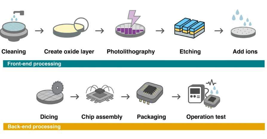
BEOL focuses on connecting those transistors into functional circuits. During this stage, multiple interconnect layers are built to route signals and distribute power throughout the chip. Although BEOL does not create the transistors, it plays an important role in signal integrity, power delivery, heat management, and overall device reliability.
After BEOL is completed, the wafer proceeds to testing, packaging, and final assembly. These final stages verify chip functionality, protect the semiconductor die, and prepare the device for installation in electronic products.
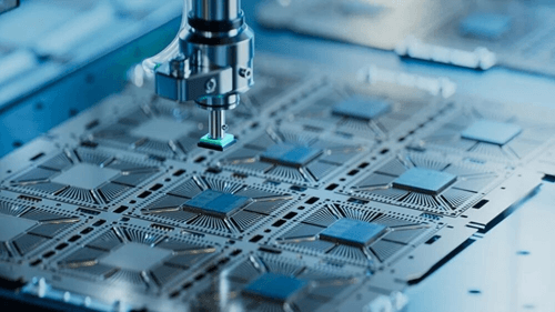
Step-By-Step IC Manufacturing Process
Wafer Manufacturing
Wafer manufacturing is the starting point of semiconductor fabrication. The wafer acts as the base platform where thousands of integrated circuits are produced simultaneously.
Crystal Growth
Crystal growth is the first major step in turning purified silicon into a usable semiconductor wafer. As shown in the image, extremely pure polysilicon is melted inside a quartz crucible using a high-temperature resistivity heater. A small seed crystal is then lowered into the silicon melt and slowly pulled upward while rotating. This controlled pulling process forms a single, continuous crystal structure known as monocrystalline silicon.
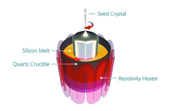
This method is called the Czochralski (CZ) process, and it is widely used in semiconductor wafer production because it can produce large, high-quality silicon ingots. During crystal growth, carefully controlled dopants such as boron, phosphorus, arsenic, or antimony may be added to adjust the electrical properties of the silicon. This is important because the wafer must have the right resistivity before transistor fabrication begins.
The final result is a large cylindrical silicon ingot that can later be sliced into thin wafers. Modern semiconductor fabs commonly use 200 mm and 300 mm wafers, while 450 mm wafer technology remains limited because of cost and manufacturing challenges. For some high-power semiconductor devices, Float-Zone (FZ) silicon may also be used because it offers very low impurity levels and excellent electrical quality.
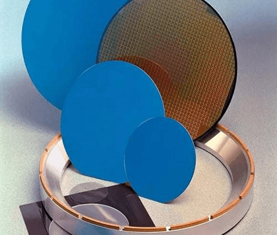
Wafer Slicing and Surface Preparation
After crystal growth, the cylindrical silicon ingot is cut into thin circular wafers using precision wire saws. As shown in the image, these wafers come in different diameters and must have a very smooth, clean, and uniform surface before they can enter the next semiconductor fabrication steps. The patterned wafer in the background also shows how the prepared wafer later becomes the base for many individual IC dies.
After slicing, each wafer goes through edge grinding, surface grinding, chemical etching, polishing, cleaning, and defect inspection. Edge grinding removes sharp edges that could crack during handling, while surface polishing creates the ultra-flat finish needed for accurate photolithography. Chemical cleaning and defect inspection help remove particles, scratches, and surface damage that could reduce yield.
This preparation stage is important because even a small surface defect can affect transistor formation in later processes. A properly sliced, polished, and inspected wafer provides the stable foundation needed for oxidation, deposition, photolithography, etching, and other advanced IC manufacturing steps.
Deposition Process
Deposition is the process of adding very thin material layers onto the wafer surface. As shown in the image, deposition can happen through different methods, depending on whether the material is formed by a chemical reaction or transferred from a solid source. These deposited layers may later become insulating films, semiconductor layers, barrier layers, or metal interconnect materials used in the IC structure.
Epitaxial Deposition
Epitaxial deposition is a special type of deposition used to grow a high-quality crystalline silicon layer on top of a silicon wafer. Unlike general film coating, the new layer follows the crystal structure of the wafer underneath it. This improves wafer quality, reduces defect density, and helps create better electrical isolation and transistor performance. Although the image mainly compares CVD and PVD, epitaxial growth is often related to CVD-based processes because gas-phase materials can be used to grow controlled silicon layers on the wafer surface.
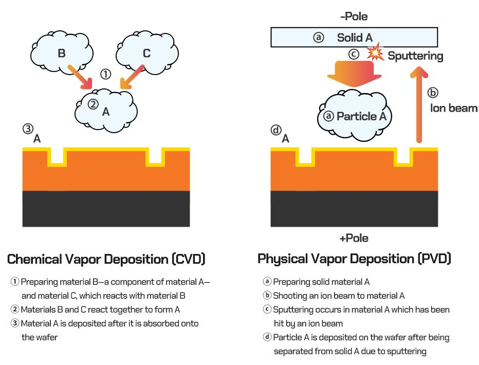
Chemical Vapor Deposition (CVD)
Chemical Vapor Deposition, or CVD, uses gas-phase materials to form a thin film on the wafer. In the image, materials B and C react together to create material A, which is then deposited onto the wafer surface. This is a good way to understand CVD: the deposited layer is not simply sprayed onto the wafer, but formed through a chemical reaction near or on the wafer surface.
CVD is widely used to deposit silicon dioxide, silicon nitride, polysilicon, and dielectric materials. These films are important for insulation, protection, transistor structures, and later patterning steps. In advanced semiconductor manufacturing, Atomic Layer Deposition, or ALD, is also used when extremely thin and uniform layers are required, especially in process nodes below 10 nm.
Physical Vapor Deposition (PVD)
Physical Vapor Deposition, or PVD, works differently from CVD. As shown on the right side of the image, an ion beam strikes a solid source material, causing particles to separate from the target through sputtering. These particles then travel toward the wafer and form a thin film on its surface.
PVD is commonly used for metal deposition, including aluminum, copper, barrier layers, and seed layers. Older IC processes often used aluminum interconnects, while many modern chips use copper because it has lower electrical resistance and supports faster signal transmission. At very advanced nodes, materials such as cobalt and ruthenium are also being studied because copper becomes harder to use efficiently at extremely small dimensions.

Thermal Oxidation
Thermal oxidation forms a silicon dioxide (SiO₂) layer directly on the silicon wafer surface. This oxide layer is widely used for insulation, transistor gate structures, surface protection, and device isolation. As shown in the image, dry oxidation produces high-quality oxide with excellent thickness control, making it suitable for thin gate dielectric applications. Wet oxidation grows oxide much faster and is commonly used when thicker oxide layers are required.
Oxide thickness directly affects transistor performance, leakage current, power consumption, and long-term reliability. If the oxide becomes too thin, leakage current and quantum tunneling effects can increase significantly. To address these challenges, advanced semiconductor nodes often use high-k dielectric materials such as hafnium oxide (HfO₂), which provide strong gate control while reducing leakage current in nanoscale transistors.
Photolithography
Photolithography transfers microscopic circuit patterns onto the wafer surface. It is widely considered the most critical step in semiconductor manufacturing because it determines transistor size and chip density.
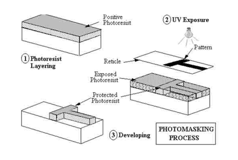
The process begins by coating the wafer with photoresist. Ultraviolet light passes through a photomask containing the circuit design, exposing selected regions of the photoresist. After development, the remaining pattern guides later etching and implantation steps.
Modern semiconductor manufacturing uses Extreme Ultraviolet (EUV) lithography for advanced nodes such as 7 nm, 5 nm, 3 nm, and beyond.
Multi-patterning is also used to create features that are smaller or denser than a single lithography exposure can easily produce. Common methods include double patterning, Self-Aligned Double Patterning (SADP), and Self-Aligned Quadruple Patterning (SAQP). These techniques split or multiply patterns across several process steps, improving pattern density and accuracy. Even with EUV lithography, multi-patterning remains important for advanced semiconductor manufacturing.
Why Smaller Nodes Are More Difficult
As semiconductor nodes shrink, manufacturing becomes significantly harder due to:
• Quantum tunneling
• Overlay accuracy limitations
• Line edge roughness
• Stochastic defects
• Increased leakage current
• Higher heat density
Smaller transistors improve performance and power efficiency, but they also require far more precise lithography systems and tighter process control.
High-NA EUV systems are now being deployed to support future 2 nm and 1 nm semiconductor manufacturing. These systems can cost hundreds of millions of dollars each.
Etching Process
Etching is the process that transfers the photolithography pattern into the actual wafer materials. After the photoresist pattern is formed, etching removes the exposed parts of thin films, such as silicon dioxide, silicon nitride, polysilicon, or metal layers. This step allows the circuit pattern to become part of the wafer structure instead of remaining only on the photoresist layer.
Modern semiconductor manufacturing mainly uses plasma-based dry etching because it provides better control for very small features. Unlike wet chemical etching, dry etching can remove materials more directionally, which helps create sharper patterns and more vertical sidewalls. This precision is important in advanced ICs, where even a small pattern error can affect transistor performance, leakage current, or production yield.
Common advanced etching methods include Reactive Ion Etching (RIE), Inductively Coupled Plasma (ICP) etching, and Atomic Layer Etching (ALE). RIE combines chemical reactions with ion bombardment to remove material accurately, while ICP etching provides high plasma density for faster and more controlled material removal. ALE removes material layer by layer with very high precision, making it useful for advanced FinFET and Gate-All-Around transistor structures where nanoscale accuracy is required.
Ion Implantation
Ion implantation is the process of adding controlled dopants into selected areas of the silicon wafer to create P-type and N-type regions. Dopants such as boron, phosphorus, and arsenic are implanted into the wafer with high precision so the transistor can control current properly. This step affects transistor speed, threshold voltage, leakage current, power efficiency, and long-term reliability, so even small errors in dopant placement or dose can reduce chip yield and performance.
Gate Formation and Transistor Fabrication
Gate formation and transistor fabrication create the active devices that perform switching operations inside an integrated circuit. After photolithography, etching, and ion implantation, the gate dielectric and gate electrode are formed to control current flow between the source and drain regions. The gate structure is then patterned, followed by the formation of source and drain regions through additional implantation processes.
As transistor dimensions continue to shrink, semiconductor manufacturers use advanced structures such as FinFET and Gate-All-Around (GAA) transistors to improve gate control, reduce leakage current, and increase performance. After fabrication, billions of transistors exist on the wafer, but they must still be connected through multiple metal interconnect layers to create complete electronic circuits.
Thermal Processing (Annealing)
Thermal processing, especially annealing, is commonly performed after ion implantation to activate the implanted dopants. During implantation, dopant atoms are placed into selected regions of the wafer, but they may not immediately sit in the correct crystal positions. Annealing uses controlled heat to move these dopants into active sites in the silicon lattice, allowing them to properly change the electrical behavior of the transistor regions.
Rapid Thermal Processing (RTP) and Rapid Thermal Annealing (RTA) are widely used because they heat the wafer for a short time at high temperature. This activates dopants while limiting unwanted dopant diffusion, which is important for maintaining small and accurate transistor features. Thermal processing can also repair implantation-related crystal damage, improve film quality, support stress engineering, and increase material stability before the next transistor fabrication steps.
Chemical Mechanical Polishing (CMP)
Chemical Mechanical Polishing, or CMP, is used to flatten the wafer surface after deposition and patterning. This is important because modern ICs contain many stacked layers, and an uneven surface can make later photolithography steps inaccurate. CMP uses polishing pads and chemical slurries to remove excess material and create a smooth, level surface for the next process.
CMP is especially important for copper interconnects, dual-damascene structures, and multi-layer routing. However, it must be carefully controlled because it can also cause defects such as dishing, erosion, and surface scratches. If these defects are not managed properly, they can reduce chip yield, affect reliability, and create problems in later manufacturing steps.
Metallization and Interconnect Formation
After transistor fabrication is completed, metal interconnect structures are formed to electrically connect billions of transistors together.
Modern semiconductor chips use multiple layers of copper routing connected through microscopic vias.
Damascene Process
The damascene process creates trenches and vias inside dielectric materials, then fills them with copper. Excess copper is removed using CMP.
Barrier Layers
Barrier metals prevent copper diffusion into surrounding semiconductor materials. Without these layers, copper contamination could damage transistor structures.
RC Delay and Electromigration
As interconnect dimensions shrink, semiconductor manufacturers face major challenges including:
• RC signal delay
• Electromigration
• Heat generation
• Signal integrity problems
Advanced BEOL routing technologies are critical for maintaining high-speed processor performance.
Wafer Metrology
Wafer metrology measures critical dimensions and physical characteristics throughout semiconductor manufacturing to ensure each process meets design specifications. Common measurements include film thickness, critical dimension (CD), overlay alignment, and surface topography. These measurements help engineers verify that deposited layers, patterned features, and lithography alignment remain within extremely tight tolerances. Modern metrology systems can measure features below 10 nm while maintaining the high throughput required for advanced semiconductor production.
Wafer Inspection
Wafer inspection is used to identify defects that can reduce yield and affect device reliability. Inspection systems look for particles, scratches, contamination, and pattern defects that may occur during fabrication. Unpatterned inspection focuses on bare wafers and non-patterned surfaces, while patterned inspection examines circuit features after lithography and etching. Modern inspection tools use optical and electron beam technologies to detect extremely small defects, allowing manufacturers to identify problems before they impact large numbers of chips.
Wafer Probe Testing
Wafer probe testing electrically tests each die before packaging. Hair-thin probes contact the chip pads to verify circuit functionality and electrical performance. Defective dies are identified before packaging to reduce production cost. AI-based analytics are increasingly used to identify systematic manufacturing problems and improve overall yield.
Packaging and Assembly
Packaging and assembly protect the finished chip and connect it to external circuits. The package shields the die from damage, moisture, contamination, and heat while allowing it to be mounted on a circuit board.
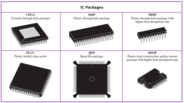
Traditional packaging methods include wire bonding, lead frames, BGA, QFN, and flip-chip packaging. These are still widely used in consumer electronics, industrial equipment, automotive systems, and communication devices because they are reliable and cost-effective.
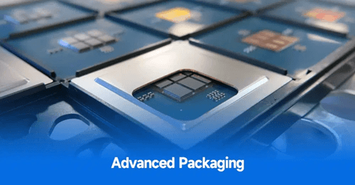
Advanced packaging is now important for AI processors, GPUs, and high-performance computing devices. Chiplet technology combines several smaller dies in one package to improve yield and allow different technologies to work together. 2.5D packaging places multiple dies on a silicon interposer for faster communication. 3D packaging stacks dies vertically using Through-Silicon Vias, or TSVs, to increase connection density and reduce package size. Hybrid bonding directly joins copper and dielectric layers, enabling very fine connections for faster and more efficient chips.
Conclusion
Understanding the integrated circuit manufacturing process provides valuable insight into how modern processors, memory devices, sensors, and communication chips are created. From a simple silicon wafer to a finished semiconductor device, every stage plays an important role in enabling the electronic products that power today's digital world.
Frequently Asked Questions [FAQ]
1. Why is photolithography considered the most critical step in semiconductor manufacturing?
Photolithography determines the size and spacing of transistor structures on the wafer. Smaller and more accurate patterns allow higher transistor density, faster processing speed, and better power efficiency. Even a tiny alignment or exposure error can reduce yield or affect chip performance.
2. Why are advanced semiconductor nodes like 3nm and 2nm more difficult to manufacture?
Smaller nodes require extremely precise process control because transistor structures become so small that issues like quantum tunneling, leakage current, overlay errors, and heat density become harder to manage. Advanced nodes also depend heavily on EUV lithography and expensive fabrication equipment.
3. How does thermal oxidation affect MOSFET performance and reliability?
Thermal oxidation forms the silicon dioxide gate layer that controls transistor switching. If the oxide layer is too thick, transistor speed decreases, but if it becomes too thin, leakage current and gate breakdown may occur. Proper oxide control is critical for balancing speed, power efficiency, and reliability.
4. Why is copper widely used in modern semiconductor interconnects instead of aluminum?
Copper has lower electrical resistance than aluminum, allowing faster signal transmission and lower power loss in advanced chips. However, copper also requires barrier layers and more complex manufacturing processes because it can diffuse into surrounding semiconductor materials.
5. Why do semiconductor fabs use extremely clean environments during production?
Modern transistor structures are measured in nanometers, so even microscopic dust particles or contamination can damage circuit patterns and reduce production yield. Cleanrooms help control particles, humidity, temperature, and chemical contamination throughout the manufacturing process.
6. How does ion implantation improve transistor performance in integrated circuits?
Ion implantation introduces controlled dopants into the wafer to create P-type and N-type regions. This process directly affects transistor switching speed, threshold voltage, leakage current, and power efficiency, making accurate dopant control essential for reliable IC performance.
7. Why do advanced AI processors rely heavily on modern packaging technologies?
AI chips generate massive amounts of data and heat, so advanced packaging technologies such as chiplets, 2.5D packaging, 3D stacking, and hybrid bonding help improve bandwidth, signal speed, power delivery, and thermal management.
Related Article
-
![How to Control DC Motors Using the L293D Motor Driver IC]() Jun 09 2026How to Control DC Motors Using the L293D Motor Driver IC
Jun 09 2026How to Control DC Motors Using the L293D Motor Driver ICControlling a motor with a microcontroller is not as simple as connecting it directly to an output pin. Most microcontrollers cannot provide enough cu...
Related products

CGA2B2X8R1H222M050BA
CAP CER 2200PF 50V X8R 0402

08055A390KAT4A
CAP CER 39PF 50V C0G/NP0 0805
08051U1R8CAT2A
CAP CER 1.8PF 100V NP0 0805
MB86R01PB-GSE1
IC SOC GRAPHIC CONTRLR 484BGA
PI74FCT16245TAEX
IC TXRX NON-INVERT 5.5V 48TSSOP
MBR4015CTLG
DIODE ARRAY SCHOTTKY 15V TO220AB
V24B8H200BL
DC DC CONVERTER 8V 200W

2MBI800U4G-120
IGBT Modules
G65SC02P-2
CMD TDIP

MAX743EWE
MAX743 DUAL OUTPUT, SWITCH-MODE

TXB0108ZXYRG4
TXB0108ZXYRG4 TI

UPD78F0537DA
UPD78F0537DA NEC
9FGV0641AKLFT
VFQFPN 5.00X5.00X0.90 MM, 0.40MM