All Categories
-
Integrated Circuits (ICs)
Integrated Circuits (ICs)
- Interface - Sensor, Capacitive Touch(642)
- Specialized ICs(12302)
- Power Management (PMIC) - Special Purpose Regulators(5644)
- Power Management (PMIC) - Voltage Regulators - Linear Regulator Controllers(793)
- Power Management (PMIC) - Voltage Regulators - Linear + Switching(1829)
- Power Management (PMIC) - Voltage Regulators - Linear, Low Drop Out (LDO) Regulators(70981)
- Power Management (PMIC) - Voltage Regulators - DC DC Switching Regulators(39569)
- Power Management (PMIC) - DC DC Switching Controllers(13507)
- Power Management (PMIC) - Voltage Reference(9453)
- Power Management (PMIC) - V/F and F/V Converters(145)
- Power Management (PMIC) - Thermal Management(592)
- Power Management (PMIC) - Supervisors(47946)
- Power Management (PMIC) - RMS to DC Converters(170)
- Power Management (PMIC) - Power Supply Controllers, Monitors(2104)
- Power Management (PMIC) - Power Over Ethernet (PoE) Controllers(1008)
- Power Management (PMIC) - Power Management - Specialized(7722)
- Power Management (PMIC) - Power Distribution Switches, Load Drivers(7706)
- Power Management (PMIC) - PFC (Power Factor Correction)(1222)
- Power Management (PMIC) - OR Controllers, Ideal Diodes(705)
- Power Management (PMIC) - Motor Drivers, Controllers(4712)
- Power Management (PMIC) - Lighting, Ballast Controllers(560)
- Power Management (PMIC) - LED Drivers(7282)
- Power Management (PMIC) - Laser Drivers(573)
- Power Management (PMIC) - Hot Swap Controllers(2816)
- Power Management (PMIC) - Gate Drivers(7083)
- Power Management (PMIC) - Full Half-Bridge (H Bridge) Drivers(1342)
- Power Management (PMIC) - Energy Metering(654)
- Power Management (PMIC) - Display Drivers(1435)
- Power Management (PMIC) - Current Regulation/Management(1481)
- Power Management (PMIC) - Battery Management(5553)
- Power Management (PMIC) - Battery Chargers(3831)
- Power Management (PMIC) - AC DC Converters, Offline Switchers(4905)
- Memory - Controllers(358)
- Memory - Configuration PROMs for FPGAs(639)
- Memory - Batteries(13)
- Memory - Memory(65694)
- Logic - Universal Bus Functions(706)
- Logic - Translators, Level Shifters(2854)
- Logic - Specialty Logic(1870)
- Logic - Signal Switches, Multiplexers, Decoders(9420)
- Logic - Shift Registers(2665)
- Logic - Parity Generators and Checkers(335)
- Logic - Multivibrators(831)
- Logic - Latches(3658)
- Logic - Gates and Inverters - Multi-Function, Configurable(1687)
- Logic - Gates and Inverters(16453)
- Logic - Flip Flops(7780)
- Logic - FIFOs Memory(4240)
- Logic - Counters, Dividers(3456)
- Logic - Comparators(592)
- Logic - Buffers, Drivers, Receivers, Transceivers(17835)
- Linear - Video Processing(2909)
- Linear - Comparators(5084)
- Linear - Analog Multipliers, Dividers(263)
- Linear - Amplifiers - Video Amps and Modules(1905)
- Linear - Amplifiers - Special Purpose(1856)
- Linear - Amplifiers - Instrumentation, OP Amps, Buffer Amps(34236)
- Linear - Amplifiers - Audio(4567)
- Interface - Voice Record and Playback(556)
- Interface - UARTs (Universal Asynchronous Receiver Transmitter)(1237)
- Interface - Telecom(4467)
- Interface - Specialized(4833)
- Interface - Signal Terminators(333)
- Interface - Signal Buffers, Repeaters, Splitters(1449)
- Interface - Serializers, Deserializers(1480)
- Interface - Sensor and Detector Interfaces(1524)
- Interface - Modules(169)
- Interface - Modems - ICs and Modules(407)
- Interface - I/O Expanders(1136)
- Interface - Filters - Active(1226)
- Interface - Encoders, Decoders, Converters(714)
- Interface - Drivers, Receivers, Transceivers(20755)
- Interface - Direct Digital Synthesis (DDS)(117)
- Interface - Controllers(3628)
- Interface - CODECS(1676)
- Interface - Analog Switches, Multiplexers, Demultiplexers(12567)
- Interface - Analog Switches - Special Purpose(2533)
- Embedded - System On Chip (SoC)(4496)
- Embedded - PLDs (Programmable Logic Device)(971)
- Embedded - Microprocessors(10083)
- Embedded - Application Specific Microcontrollers(2275)
- Embedded - Microcontrollers(99285)
- Embedded - Microcontrollers, Microprocessor, FPGA Modules(1527)
- Embedded - FPGAs (Field Programmable Gate Array) with Microcontrollers(81)
- Embedded - FPGAs (Field Programmable Gate Array)(27747)
- Embedded - DSP (Digital Signal Processors)(4081)
- Embedded - CPLDs (Complex Programmable Logic Devices)(5187)
- Data Acquisition - Touch Screen Controllers(1210)
- Data Acquisition - Digital to Analog Converters (DAC)(14419)
- Data Acquisition - Digital Potentiometers(6250)
- Data Acquisition - Analog to Digital Converters (ADC)(17776)
- Data Acquisition - Analog Front End (AFE)(787)
- Data Acquisition - ADCs/DACs - Special Purpose(3043)
- Clock/Timing - Real Time Clocks(2446)
- Clock/Timing - Programmable Timers and Oscillators(23469)
- Clock/Timing - IC Batteries(4)
- Clock/Timing - Delay Lines(1049)
- Clock/Timing - Clock Generators, PLLs, Frequency Synthesizers(32775)
- Clock/Timing - Clock Buffers, Drivers(4568)
- Clock/Timing - Application Specific Clock/Timing(8652)
- Audio Special Purpose(1564)
Relevant Manufacturer


-
Discrete Semiconductor Products
Discrete Semiconductor Products
- Current Regulation - Diodes, Transistors(1090)
- Transistors - Special Purpose(226)
- Transistors - Programmable Unijunction(48)
- Transistors - JFETs(1558)
- Transistors - IGBTs - Single(4799)
- Transistors - IGBTs - Modules(63420)
- Transistors - IGBTs - Arrays(26)
- Transistors - FETs, MOSFETs - Single(48330)
- Transistors - FETs, MOSFETs - RF(4903)
- Transistors - FETs, MOSFETs - Arrays(6641)
- Transistors - Bipolar (BJT) - Single, Pre-Biased(4539)
- Transistors - Bipolar (BJT) - Single(25800)
- Transistors - Bipolar (BJT) - RF(2087)
- Transistors - Bipolar (BJT) - Arrays, Pre-Biased(2115)
- Transistors - Bipolar (BJT) - Arrays(2310)
- Thyristors - TRIACs(4044)
- Thyristors - SCRs - Modules(3967)
- Thyristors - SCRs(5436)
- Thyristors - DIACs, SIDACs(319)
- Power Driver Modules(1627)
- Diodes - Zener - Single(87483)
- Diodes - Zener - Arrays(2619)
- Diodes - Variable Capacitance (Varicaps, Varactors)(1200)
- Diodes - RF Diodes(2753)
- Diodes - Rectifiers - Single(67528)
- Diodes - Rectifiers - Arrays(20581)
- Diodes - Bridge Rectifiers(11700)
Relevant Manufacturer


-
RF and Wireless
RF and Wireless
- Subscriber Identification Module (SIM) Cards(77)
- RF Circulators and Isolators(1742)
- RFID, RF Access, Monitoring ICs(1550)
- RFID Transponders, Tags(747)
- RFID Reader Modules(464)
- RFID Evaluation and Development Kits, Boards(30)
- RFID Antennas(329)
- RFI and EMI - Shielding and Absorbing Materials(6444)
- RFI and EMI - Contacts, Fingerstock and Gaskets(7497)
- RF Transmitters(668)
- RF Transceiver Modules and Modems(6900)
- RF Transceiver ICs(4169)
- RF Switches(9276)
- RF Shields(16401)
- RF Receivers(1998)
- RF Receiver, Transmitter, and Transceiver Finished Units(2763)
- RF Power Dividers/Splitters(1223)
- RF Power Controller ICs(86)
- RF Modulators(710)
- RF Mixers(2800)
- RF Misc ICs and Modules(3276)
- RF Front End (LNA + PA)(419)
- RF Evaluation and Development Kits, Boards(747)
- RF Directional Coupler(2718)
- RF Multiplexers(1464)
- RF Detectors(412)
- RF Demodulators(249)
- RF Antennas(12319)
- RF Amplifiers(19651)
- Balun(1496)
- Attenuators(4852)
Relevant Manufacturer


-
Optoelectronics
Optoelectronics
- Optomechanical(480)
- Lighting Fixtures(125)
- Laser Diodes, Laser Modules - Laser Delivery, Laser Fibers(345)
- HeNe Laser Systems(31)
- HeNe Laser Heads(27)
- Display Backlights(93)
- Xenon Lighting(387)
- Touch Screen Overlays(453)
- Panel Indicators, Pilot Lights(75729)
- Remote Phosphor Light Source(269)
- Reflectors(665)
- Light Pipes(5384)
- Lenses(4951)
- Spacers, Standoffs(2718)
- Lamp Replacements(29718)
- Circuit Board Indicators, Arrays, Light Bars, Bar Graphs(9083)
- LED Thermal Products(667)
- LED Lighting Kits(64)
- LED White Lighting(37580)
- LED Color Lighting(4728)
- LED COBs, Engines, Modules, Strips(28735)
- LED Indication - Discrete(27601)
- Laser Diodes, Modules(1553)
- Incandescent, Neon Lamps(311004)
- Cold Cathode Fluorescent (CCFL) & UV Lamps(164)
- Ballasts, Inverters(7728)
- LED Emitters - Infrared, UV, Visible(3871)
- Fiber Optic Transmitters - Drive Circuitry Integrated(4085)
- Fiber Optic Transmitters - Discrete(350)
- Fiber Optic Transceiver Modules(18758)
- Fiber Optic Switches, Multiplexers, Demultiplexers(1387)
- Fiber Optic Receivers(695)
- Fiber Optic Attenuators(654)
- Electroluminescent(102)
- Display, Monitor - LCD Driver/Controller(98)
- Vacuum Fluorescent (VFD)(249)
- LED Dot Matrix and Cluster(865)
- LED Character and Numeric(5421)
- LCD, OLED, Graphic(4654)
- LCD, OLED Character and Numeric(2202)
- Display Bezels, Lenses(88)
- LED Addressable, Specialty(458)
Relevant Manufacturer


-
Sensors, Transducers
Sensors, Transducers
- Industrial Sensors - Ultrasonic Receivers, Transmitters - Industrial(115)
- Industrial Sensors - Thermostats - Mechanical - Industrial(3103)
- Industrial Sensors - Temperature Sensors - Analog and Digital Output - Industrial(209)
- Industrial Sensors - Proximity Sensors - Industrial(13611)
- Industrial Sensors - Pressure Sensors, Transducers - Industrial(26503)
- Optical Sensors - Photonics - Counters, Detectors, SPCM (Single Photon Counting Module)(751)
- Optical Sensors - Camera Modules(875)
- Industrial Sensors - Position, Proximity, Speed (Modules) - Industrial(554)
- Industrial Sensors - Force Sensors, Load Cells - Industrial(346)
- Industrial Sensors - Flow Sensors - Industrial(151)
- Industrial Sensors - Float, Level Sensors - Industrial(310)
- Industrial Sensors - Encoders - Industrial(4980)
- Industrial Sensors - Color Sensors - Industrial(50)
- Touch Sensors(100)
- Ultrasonic Receivers, Transmitters(2421)
- Temperature Sensors - Thermostats - Solid State(1096)
- Temperature Sensors - Thermostats - Mechanical(3397)
- Temperature Sensors - Thermocouples, Temperature Probes(1921)
- Temperature Sensors - RTD (Resistance Temperature Detector)(1525)
- Temperature Sensors - PTC Thermistors(2273)
- Temperature Sensors - NTC Thermistors(13259)
- Temperature Sensors - Analog and Digital Output(3928)
- Strain Gauges(1399)
- Specialized Sensors(1861)
- Solar Cells(503)
- Shock Sensors(84)
- Sensor Interface - Junction Blocks(2519)
- Sensor Cable - Assemblies(22011)
- Proximity/Occupancy Sensors - Finished Units(725)
- Proximity Sensors(2860)
- Pressure Sensors, Transducers(11317)
- Position Sensors - Angle, Linear Position Measuring(6022)
- Optical Sensors - Reflective - Logic Output(194)
- Optical Sensors - Reflective - Analog Output(432)
- Optical Sensors - Phototransistors(1027)
- Optical Sensors - Photointerrupters - Slot Type - Transistor Output(1427)
- Optical Sensors - Photointerrupters - Slot Type - Logic Output(1215)
- Industrial Sensors - Photoelectric, Industrial(16763)
- Optical Sensors - Photodiodes(1543)
- Optical Sensors - Photo Detectors - Remote Receiver(2605)
- Optical Sensors - Photo Detectors - Logic Output(146)
- Optical Sensors - Photo Detectors - CdS Cells(74)
- Optical Sensors - Distance Measuring(377)
- Optical Sensors - Ambient Light, IR, UV Sensors(1305)
- Multifunction(558)
- Motion Sensors - Vibration Sensors(337)
- Motion Sensors - Tilt Switches(67)
- Motion Sensors - Optical Motion Sensors(719)
- Motion Sensors - Inclinometers(175)
- Motion Sensors - IMUs (Inertial Measurement Units)(416)
- Motion Sensors - Gyroscopes(214)
- Motion Sensors - Accelerometers(1911)
- Magnets - Sensor Matched Magnets(119)
- Magnets - Multi Purpose Magnets(1965)
- Magnetic Sensors - Switches (Solid State)(3700)
- Magnetic Sensors - Position, Proximity, Speed (Modules)(5199)
- Magnetic Sensors - Linear, Compass (ICs)(1247)
- Magnetic Sensors - Compass, Magnetic Field (Modules)(35)
- LVDT Transducers (Linear Variable Differential Transformer)(204)
- IrDA Transceiver Modules(196)
- Optical Sensors - Image Sensors, Camera(2235)
- Humidity, Moisture Sensors(1425)
- Gas Sensors(1217)
- Force Sensors, Load Cells(188)
- Flow Sensors(550)
- Float, Level Sensors(1343)
- Encoders(6357)
- Particle, Dust Sensors(43)
- Current Sensors(3455)
- Color Sensors(85)
- Sensor, Transducer Amplifiers(1905)
Relevant Manufacturer


-
Connectors, Interconnects
Connectors, Interconnects
- USB, DVI, HDMI Connectors(446)
- Solid State Lighting Connectors(555)
- Sockets for ICs, Transistors(953)
- Pluggable Connectors(1221)
- Photovoltaic (Solar Panel) Connectors(136)
- Fiber Optic Connectors(370)
- FFC, FPC (Flat Flexible) Connectors(761)
- D-Sub, D-Shaped Connectors(2887)
- Coaxial Connectors (RF)(2389)
- Circular Connectors(14162)
- Blade Type Power Connectors(273)
- AC Power Connectors - Plugs and Receptacles(2597)
- USB, DVI, HDMI Connectors - USB, DVI, HDMI Connector Adapters(572)
- USB, DVI, HDMI Connectors - USB, DVI, HDMI Connector Assemblies(4298)
- Terminals - Wire to Board Connectors(217)
- Terminals - Wire Splice Connectors(4322)
- Terminals - Wire Pin Connectors(328)
- Terminals - Turret Connectors(1273)
- Terminals - Specialized Connectors(2042)
- Terminals - Spade Connectors(3902)
- Terminals - Solder Lug Connectors(345)
- Terminals - Screw Connectors(745)
- Terminals - Ring Connectors(12596)
- Terminals - Lugs(4747)
- Terminals - Quick Connects, Quick Disconnect Connectors(8514)
- Terminals - PC Pin, Single Post Connectors(3776)
- Terminals - PC Pin Receptacles, Socket Connectors(5883)
- Terminals - Magnetic Wire Connectors(1653)
- Terminals - Knife Connectors(112)
- Terminals - Housings, Boots(2850)
- Terminals - Foil Connectors(108)
- Terminals - Barrel, Bullet Connectors(1107)
- Terminals - Terminal Adapters(137)
- Terminal Strips and Turret Boards(1159)
- Terminal Junction Systems(2533)
- Terminal Blocks - Wire to Board(43615)
- Terminal Blocks - Specialized(3722)
- Terminal Blocks - Power Distribution(847)
- Terminal Blocks - Panel Mount(1359)
- Terminal Blocks - Interface Modules(1819)
- Terminal Blocks - Headers, Plugs and Sockets(119920)
- Terminal Blocks - Din Rail, Channel(9373)
- Terminal Blocks - Terminal Block Contacts(65)
- Terminal Blocks - Barrier Blocks(47517)
- Terminal Blocks - Terminal Block Adapters(1059)
- Solid State Lighting Connectors - Solid State Lighting Connector Contacts(271)
- Solid State Lighting Connectors - Solid State Lighting Connector Assemblies(1344)
- Sockets for ICs, Transistors - Socket Adapters(275)
- Sockets for ICs, Transistors - IC Sockets(22148)
- Shunts, Jumpers(907)
- Rectangular Connectors - Spring Loaded(7721)
- Rectangular Connectors - Rectangular Connector Housings(43023)
- Rectangular Connectors - Headers, Specialty Pin(6129)
- Rectangular Connectors - Headers, Receptacles, Female Sockets(229601)
- Rectangular Connectors - Headers, Male Pins(543338)
- Rectangular Connectors - Free Hanging, Panel Mount(30142)
- Rectangular Connectors - Rectangular Connector Contacts(10681)
- Rectangular Connectors - Board In, Direct Wire to Board(2432)
- Rectangular Connectors - Rectangular Connector Adapters(475)
- Rectangular - Board to Board Connectors - Headers, Receptacles, Female Sockets(9)
- Rectangular - Board to Board Connectors - Headers, Male Pins(2)
- Rectangular Connectors - Board Spacers, Stackers (Board to Board)(238901)
- Rectangular Connectors - Arrays, Edge Type, Mezzanine (Board to Board)(37853)
- AC Power Connectors - Power Entry Modules (PEM)(10310)
- Pluggable Connectors - Pluggable Connector Assemblies(6049)
- Photovoltaic (Solar Panel) Connectors - Photovoltaic (Solar Panel) Connector Contacts(77)
- Photovoltaic (Solar Panel) Connectors - Photovoltaic (Solar Panel) Connector Assemblies(504)
- Modular/Ethernet Connectors - Modular/Ethernet Connector Wiring Blocks(99)
- Modular/Ethernet Connectors - Modular/Ethernet Connector (RJ45, RJ11) Plugs(1674)
- Modular/Ethernet Connectors - Modular/Ethernet Connector Plug Housings(181)
- Modular/Ethernet Connectors - Modular/Ethernet Connector (RJ45) Jacks With Magnetics(10152)
- Modular/Ethernet Connectors - Modular/Ethernet Connector (RJ45, RJ11) Jacks(23416)
- Modular/Ethernet Connectors - Modular/Ethernet Connector Adapters(855)
- Memory Connectors - PC Cards - Adapters(21)
- Memory Connectors - PC Card Sockets(3299)
- Memory Connectors - Inline Module Sockets(3390)
- LGH Connectors(764)
- Keystone Connectors - Keystone Inserts(2758)
- Keystone Connectors - Keystone Faceplates, Frames(1926)
- Heavy Duty Connectors - Heavy Duty Connector Inserts, Modules(4190)
- Heavy Duty Connectors - Heavy Duty Connector Housings, Hoods, Bases(17226)
- Heavy Duty Connectors - Heavy Duty Connector Frames(523)
- Heavy Duty Connectors - Heavy Duty Connector Contacts(1832)
- Heavy Duty Connectors - Heavy Duty Connector Assemblies(671)
- Fiber Optic Connectors - Fiber Optic Connector Housings(919)
- Fiber Optic Connectors - Fiber Optic Connector Adapters(4455)
- Fiber Optic Connectors - Fiber Optic Connector Assemblies(3001)
- FFC, FPC (Flat Flexible) Connectors - FFC, FPC (Flat Flexible) Connector Housings(652)
- FFC, FPC (Flat Flexible) Connectors - FFC, FPC (Flat Flexible) Connector Contacts(202)
- FFC, FPC (Flat Flexible) Connectors - FFC, FPC (Flat Flexible) Connector Assemblies(18691)
- D-Sub, D-Shaped Connectors - D-Sub, D-Shaped Connector Terminators(47)
- D-Sub, D-Shaped Connectors - D-Sub, D-Shaped Connector Housings(12238)
- D-Sub, D-Shaped Connectors - D-Sub, D-Shaped Connector Contacts(2714)
- D-Sub, D-Shaped Connectors - D-Sub, D-Shaped Connector Backshells, Hoods(5995)
- D-Sub, D-Shaped Connectors - D-Sub, D-Shaped Connector Adapters(1304)
- D-Sub, D-Shaped Connectors - D-Sub Connector Assemblies(141346)
- D-Sub, D-Shaped Connectors - Centronics Connectors(8770)
- Contacts - Contacts, Spring Loaded (Pogo Pins), and Pressure(630)
- Contacts - Multi Purpose(6196)
- Contacts - Leadframe(122)
- Coaxial Connectors (RF) - Coaxial Connector (RF) Terminators(1231)
- Coaxial Connectors (RF) - Coaxial Connector (RF) Contacts(480)
- Coaxial Connectors (RF) - Coaxial Connector (RF) Adapters(6386)
- Coaxial Connectors (RF) - Coaxial Connector (RF) Assemblies(25734)
- Circular Connectors - Circular Connector Housings(441226)
- Circular Connectors - Circular Connector Contacts(4737)
- Circular Connectors - Backshells and Cable Clamps(53692)
- Circular Connectors - Circular Connector Adapters(8839)
- Circular Connectors - Circular Connector Assemblies(1196254)
- Card Edge Connectors - Card Edge Connector Housings(469)
- Card Edge Connectors - Edgeboard Connectors(672683)
- Card Edge Connectors - Card Edge Connector Contacts(325)
- Card Edge Connectors - Card Edge Connector Adapters(73)
- Blade Type Power Connectors - Blade Type Power Connector Housings(837)
- Blade Type Power Connectors - Blade Type Power Connector Contacts(393)
- Blade Type Power Connectors - Blade Type Power Connector Assemblies(4163)
- Between Series Adapters(649)
- Barrel Connectors - Power Connectors(935)
- Barrel Connectors - Audio Connectors(2432)
- Barrel Connectors - Barrel Connector Adapters(92)
- Banana and Tip Connectors - Jacks, Plugs(1644)
- Banana and Tip Connectors - Binding Posts(239)
- Banana and Tip Connectors - Banana and Tip Connector Adapters(75)
- Backplane Connectors - Specialized(45586)
- Backplane Connectors - Backplane Connector Housings(6863)
- Backplane Connectors - Hard Metric, Standard(6297)
- Backplane Connectors - DIN 41612(9408)
- Backplane Connectors - Backplane Connector Contacts(3583)
- Backplane Connectors - ARINC Inserts(2357)
- Backplane Connectors - ARINC(3789)
Relevant Manufacturer


-
Resistors
-
Capacitors
Capacitors
- Aluminum Capacitors(16817)
- Trimmers, Variable Capacitors(3151)
- Thin Film Capacitors(3473)
- Tantalum Capacitors(136103)
- Tantalum - Polymer Capacitors(9778)
- Silicon Capacitors(320)
- Niobium Oxide Capacitors(330)
- Mica and PTFE Capacitors(9101)
- Film Capacitors(150406)
- Electric Double Layer Capacitors (EDLC), Supercapacitors(2782)
- Ceramic Capacitors(833829)
- Capacitor Networks, Arrays(2383)
- Aluminum Electrolytic Capacitors(125325)
- Aluminum - Polymer Capacitors(7544)
Relevant Manufacturer


-
Transformers
-
Isolators
Isolators
Relevant Manufacturer


-
Crystals, Oscillators, Resonators
-
Switches
Switches
- Interlock Switches(2893)
- Emergency Stop (E-Stop) Switches(1160)
- Cable Pull Switches(571)
- Toggle Switches(33608)
- Thumbwheel Switches(742)
- Tactile Switches(14263)
- Limit Switches(28077)
- Slide Switches(5166)
- Selector Switches(9720)
- Rotary Switches(13850)
- Rocker Switches(53790)
- Pushbutton Switches - Hall Effect(127)
- Pushbutton Switches(190826)
- Programmable Display Switches(39)
- Navigation Switches, Joystick(1882)
- Magnetic, Reed Switches(1399)
- Keypad Switches(637)
- Keylock Switches(3684)
- DIP Switches(7747)
- Configurable Switch Components - Configurable Switch Lens(1435)
- Configurable Switch Components - Configurable Switch Illumination Sources(1236)
- Configurable Switch Components - Configurable Switch Contact Blocks(1401)
- Configurable Switch Components - Configurable Switch Bodies(16077)
- Disconnect Switch Components(2567)
Relevant Manufacturer


-
Relays
Relays
- Safety Relays(1310)
- Reed Relays(1735)
- High Frequency (RF) Relays(1190)
- Contactors (Solid State)(686)
- Contactors (Electromechanical)(11952)
- Automotive Relays(1881)
- Solid State Relays (SSR)(10652)
- Signal Relays, Up to 2 Amps(9149)
- Relay Sockets(2075)
- Power Relays, Over 2 Amps(31604)
- I/O Relay Modules(712)
- I/O Relay Modules - Input(2)
- I/O Relay Module Racks(247)
Relevant Manufacturer


Select Language
Current Language
English
- English
- Deutsch
- Italia
- Français
- 日本語
- 한국의
- русский
- Svenska
- Nederland
- español
- Português
- polski
- Suomi
- Gaeilge
- Slovenská
- Slovenija
- Čeština
- Melayu
- Magyarország
- Hrvatska
- Dansk
- românesc
- Indonesia
- Ελλάδα
- Български език
- Afrikaans
- IsiXhosa
- isiZulu
- lietuvių
- Maori
- Kongeriket
- Монголулс
- O'zbek
- Tiếng Việt
- हिंदी
- اردو
- Kurdî
- Català
- Bosna
- Euskera
- العربية
- فارسی
- Corsa
- Chicheŵa
- עִבְרִית
- Latviešu
- Hausa
- Беларусь
- አማርኛ
- Republika e Shqipërisë
- Eesti Vabariik
- íslenska
- မြန်မာ
- Македонски
- Lëtzebuergesch
- საქართველო
- Cambodia
- Pilipino
- Azərbaycan
- ພາສາລາວ
- বাংলা ভাষার
- پښتو
- malaɡasʲ
- Кыргыз тили
- Ayiti
- Қазақша
- Samoa
- සිංහල
- ภาษาไทย
- Україна
- Kiswahili
- Cрпски
- Galego
- नेपाली
- Sesotho
- Тоҷикӣ
- Türk dili
- ગુજરાતી
- ಕನ್ನಡkannaḍa
- मराठी
How Does the JRC4558 Operational Amplifier Work?
Time: June 10th, 2026
Browse: 199
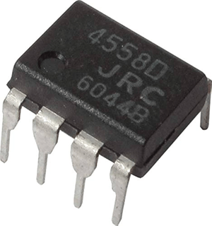
The JRC4558 dual operational amplifier is designed to amplify and process small electrical signals. It contains two independent op-amps in one package, making it useful for circuits that need more than one signal-processing stage without adding extra ICs. This article explains the JRC4558’s key features, specifications, pin functions, working principle, circuit behavior, package dimensions, and comparison with other popular op-amps.
Catalog
JRC4558 Dual Operational Amplifier
The JRC4558 Dual Operational Amplifier is an integrated circuit that contains two independent operational amplifiers in one package. It is designed to amplify small analog signals and support stable signal processing in electronic circuits.
Each amplifier inside the JRC4558 has high voltage gain and can be configured with external components to control gain, feedback, and signal response. Its dual-channel structure helps reduce component count and saves PCB space compared with using two separate op-amp ICs.
The JRC4558 is valued for its simple design, stable operation, wide availability, and cost-effective performance. While newer op-amps may offer lower noise or faster response, the JRC4558 remains a practical choice for many general analog circuit designs.
If you are interested in purchasing the JRC4558 dual operational amplifier, feel free to contact us for pricing and availability.
Features and Specifications of the JRC4558
|
Parameter |
Specification |
|
Device Type |
Dual Operational
Amplifier |
|
Number of
Amplifiers |
2 |
|
Frequency
Compensation |
Internally
compensated |
|
Latch-Up
Protection |
No latch-up |
|
Common-Mode
Voltage Range |
Large
common-mode input range |
|
Differential
Input Voltage Range |
Wide
differential input range |
|
Channel Matching |
Gain and phase
matched amplifiers |
|
Input Transistor
Type |
Low-noise input
transistors |
|
Pin
Compatibility |
MC1458, LM358
compatible |
|
Supply Voltage
(Max) |
±22 V |
|
Differential
Input Voltage (Max) |
±18 V |
|
Input Voltage
(Max) |
±15 V |
|
Operating
Temperature Range |
-20°C to +85°C |
|
Storage
Temperature Range |
-65°C to +150°C |
|
Power
Dissipation (PDIP-8) |
600 mW |
|
Power
Dissipation (SOP-8) |
400 mW |
|
Supply Current |
2.3 mA to 4.5 mA |
|
Input Offset
Voltage |
2 – 6 mV |
|
Input Offset
Current |
5 nA - 200 nA |
|
Input Bias
Current |
30 – 500 nA |
|
Large Signal
Voltage Gain (Min) |
20 V/mV - 200
V/mV |
|
Common-Mode
Input Voltage Range (Min) |
±12 V - ±13 V |
|
Common-Mode
Rejection Ratio |
70 – 90 dB |
|
Power Supply
Rejection Ratio |
76 – 90 dB |
|
Output Voltage
Swing (Typ) |
±12 V |
|
Output Voltage
Swing (Max) |
±14 V |
|
Power
Consumption (Typ) |
70 mW |
|
Power
Consumption (Max) |
170 mW |
|
Slew Rate |
1.2 - 2.2 V/μs |
|
Rise Time (Typ) |
0.3 μs |
|
Overshoot (Typ) |
15% |
|
Input Resistance
(Min) |
0.3 - 2MΩ |
|
Output
Resistance (Typ) |
75 Ω |
|
Total Harmonic
Distortion (Typ) |
0.008% |
|
Channel
Separation (Typ) |
120 dB |
|
Unity Gain
Bandwidth |
2.0 to 2.8 MHz |
|
Package Options |
PDIP-8, SOP-8 |
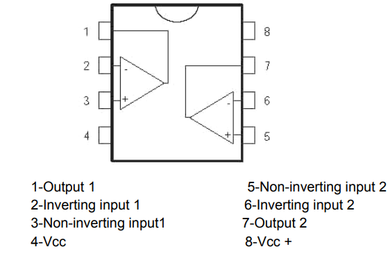
JRC4558 Pinout and Pin Functions
|
Pin
No. |
Pin
Name |
Function
Description |
|
1 |
Output 1 |
Output terminal
of the first operational amplifier. The amplified signal from Op-Amp 1
appears at this pin. |
|
2 |
Inverting Input
1 (-) |
Inverting input
of the first amplifier. A signal applied here produces an output that is 180°
out of phase with the input. |
|
3 |
Non-Inverting
Input 1 (+) |
Non-inverting
input of the first amplifier. A signal applied here produces an output that
is in phase with the input. |
|
4 |
VCC− |
Negative power
supply terminal. In dual-supply circuits, this pin is connected to the
negative voltage rail. |
|
5 |
Non-Inverting
Input 2 (+) |
Non-inverting
input of the second amplifier. Signals applied to this pin are amplified
without phase inversion. |
|
6 |
Inverting Input
2 (-) |
Inverting input
of the second amplifier. Signals applied here are amplified with phase
inversion. |
|
7 |
Output 2 |
Output terminal
of the second operational amplifier. The amplified signal from Op-Amp 2
appears at this pin. |
|
8 |
VCC+ |
Positive power
supply terminal. This pin supplies operating voltage to both amplifiers
inside the IC. |
How the JRC4558 Amplifies and Processes Analog Signals
The JRC4558 amplifies analog signals through several internal transistor stages that work together to provide voltage gain, signal conditioning, and output drive capability. As shown in the internal circuit diagram, the amplification process begins at the differential input stage, where transistors compare the voltage difference between the non-inverting (+IN) and inverting (-IN) inputs. Rather than amplifying each input independently, the device amplifies the difference between the two signals. This differential operation helps reject common-mode noise and improves overall signal accuracy.
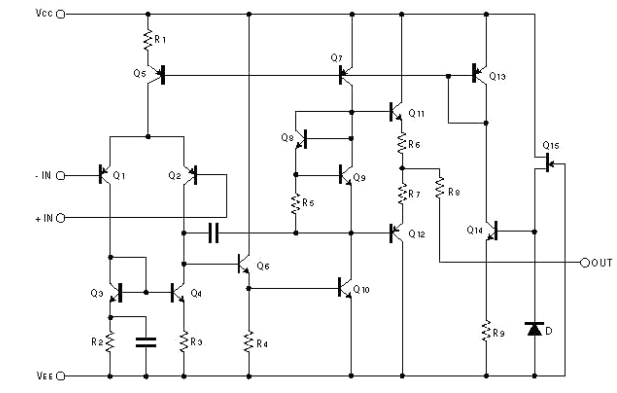
After the input signal is detected, it passes through intermediate transistor stages that provide most of the voltage amplification. These stages increase the signal amplitude while maintaining linear operation. The JRC4558 also includes internal frequency compensation, which helps stabilize the amplifier and reduces the risk of unwanted oscillation. This compensation allows the device to operate reliably in a wide range of circuit configurations without requiring external compensation components.
The amplified signal is then delivered to the output stage, where additional transistors provide the current needed to drive external loads. In most circuits, a portion of the output signal is fed back to the inverting input through a feedback network. This negative feedback controls the amplifier gain, improves stability, reduces distortion, and helps achieve the desired circuit performance. Through this multi-stage architecture, the JRC4558 can accurately process and amplify low-level analog signals while maintaining stable operation and good signal quality.
Common JRC4558 Circuit Applications
The circuit diagram shows a practical audio signal processing circuit built around the dual amplifiers inside the JRC4558. Both operational amplifiers are used together to process the input signal before delivering the final output. The first amplifier stage receives the input signal through resistor R1 and uses a feedback network to control gain and signal behavior. Diodes D1 and D2 are connected in the feedback path and act as clipping elements. When the signal amplitude exceeds the forward voltage of the diodes, they begin conducting and limit the signal peaks. This creates a controlled clipping effect that modifies the waveform and introduces harmonic distortion.
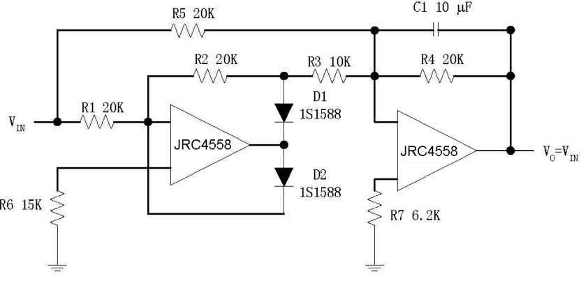
The clipped signal is then passed to the second JRC4558 amplifier stage through a network of resistors and capacitor C1. This stage provides additional amplification, filtering, and signal shaping. The resistor network determines the gain and frequency response, while capacitor C1 helps control the circuit's tonal characteristics by affecting how different frequencies are processed. The second amplifier also buffers the signal, helping maintain a stable output level.
In real-world applications, this type of circuit is commonly used for analog signal conditioning and audio processing. The first op-amp stage performs amplification and clipping, while the second stage refines the processed signal and drives the output. This demonstrates how the JRC4558 can be used not only as a simple amplifier but also as an active signal-processing device capable of combining amplification, feedback control, filtering, and waveform modification within a single circuit design.
The diagram also illustrates one of the key advantages of the JRC4558's dual-op-amp architecture. Since two independent amplifiers are available in the same package, designers can create multiple signal-processing stages without requiring additional ICs. This reduces component count, saves board space, simplifies circuit design, and lowers overall system cost while maintaining reliable analog performance.
JRC4558 vs Other Popular Operational Amplifiers
|
Parameter |
JRC4558 |
LM358 |
NE5532 |
TL072 |
|
Number of
Amplifiers |
2 |
2 |
2 |
2 |
|
Supply Voltage
Range |
±5V to ±15V |
3V to 32V /
±1.5V to ±16V |
±3V to ±20V |
±5V to ±18V |
|
Unity Gain
Bandwidth |
2.8 MHz |
1 MHz |
10 MHz |
3 MHz |
|
Slew Rate |
2.2 V/μs |
0.3 V/μs |
9 V/μs |
13 V/μs |
|
Input Offset
Voltage (Typ) |
2 mV |
2 mV |
0.5 mV |
3 mV |
|
Input Bias
Current (Typ) |
30 nA |
20 nA |
200 nA |
65 pA |
|
Input Resistance
(Typ) |
2 MΩ |
10 MΩ |
300 kΩ |
10¹² Ω |
|
Supply Current
(Typ) |
2.3 mA |
0.7 mA |
8 mA |
2.8 mA |
|
Output Voltage
Swing (Typ) |
±12 V |
VCC − 1.5 V |
±13 V |
±13.5 V |
|
THD (Typ) |
0.008% |
0.02% |
0.0005% |
0.003% |
|
Noise Density
(Typ) |
~8 nV/√Hz |
~40 nV/√Hz |
~5 nV/√Hz |
~18 nV/√Hz |
|
Common-Mode
Rejection Ratio (Typ) |
90 dB |
85 dB |
100 dB |
100 dB |
|
Power Supply
Rejection Ratio (Typ) |
90 dB |
100 dB |
100 dB |
100 dB |
|
Operating
Temperature Range |
-20°C to +85°C |
0°C to +70°C |
0°C to +70°C |
-40°C to +85°C |
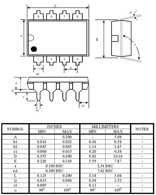
JRC4558 Mechanical Dimensions
Conclusion
The JRC4558 continues to provide reliable signal amplification for a wide range of analog circuit designs. Understanding its specifications, pin functions, internal operation, and real-world circuit behavior allows you to use the device more effectively and avoid common design limitations. The dual-op-amp architecture also enables multiple signal-processing stages within a single package, helping reduce component count and simplify circuit layouts.
Frequently Asked Questions [FAQ]
1. Can the JRC4558 operate from a single power supply instead of dual supplies?
Yes. The JRC4558 can operate from a single supply if a suitable bias voltage is created for the input and output stages. However, dual-supply operation often provides greater output swing and simplifies signal handling.
2. How does the slew rate of the JRC4558 affect circuit performance?
The 2.2 V/μs slew rate limits how quickly the output can respond to rapid input changes. For most low-frequency analog circuits this is sufficient, but high-speed applications may require a faster op-amp.
3. What happens if the common-mode input voltage exceeds the specified range?
Exceeding the common-mode range can cause distortion, reduced gain accuracy, or improper amplifier operation. Inputs should remain within the recommended limits for reliable performance.
4. Why is negative feedback important when using the JRC4558?
Negative feedback stabilizes the amplifier, controls gain, improves linearity, reduces distortion, and helps maintain predictable circuit behavior.
5. How does the JRC4558 compare with modern low-noise op-amps?
Modern devices often provide lower noise, higher bandwidth, and faster slew rates. However, the JRC4558 remains attractive for designs that prioritize simplicity, availability, and cost-effectiveness.
6. What factors should be considered when replacing a JRC4558 with another op-amp?
Engineers should verify supply voltage requirements, pin compatibility, bandwidth, slew rate, input characteristics, and circuit stability before selecting a replacement.
7. Why does the JRC4558 contain two operational amplifiers in one package?
The dual-op-amp design allows multiple amplification or signal-processing stages to be implemented using a single IC, reducing PCB space and component count.
8. How can excessive noise be reduced in a JRC4558 circuit?
Proper grounding, short signal paths, clean power supplies, decoupling capacitors, and appropriate feedback network design can significantly reduce unwanted noise.
Related Article
-
![CAN Bus Transceiver Failure Diagnosis and Troubleshooting Steps]() Jun 10 2026CAN Bus Transceiver Failure Diagnosis and Troubleshooting Steps
Jun 10 2026CAN Bus Transceiver Failure Diagnosis and Troubleshooting StepsCAN bus communication is widely used in automotive systems, industrial automation, robotics, medical equipment, and embedded control networks. When a ... -
![IR2110-Based High-Frequency Inverter Design and Implementation]() Jun 10 2026IR2110-Based High-Frequency Inverter Design and Implementation
Jun 10 2026IR2110-Based High-Frequency Inverter Design and ImplementationA high-frequency inverter is an important circuit used to convert DC power into AC power for electronic and power control applications. In this design...

Related products
MCP41010-I/P
IC DGTL POT 10KOHM 256TAP 8DIP

LTC2640AITS8-HZ12#TRPBF
IC DAC 12BIT VOUT W/REF TSOT23-8
EP3C16M164I7N
IC FPGA 92 I/O 164MBGA

S9KEAZ128AVLH
IC MCU 32BIT 128KB FLASH 64LQFP

OPA4330AIDR
IC OPAMP ZERO-DRIFT 4CIRC 14SOIC

S200-50
RF TRANS NPN 110V 30MHZ 55HX

W81E381D
winbond LQFP-48

FC1610-BC-AJ
FC1610-BC-AJ LEXAR
MC145158P1
MC145158P1 MOT
T491C685M025AT42807333
CAP TANT 6.8UF 20% 25V 2312
T491D107M010ZTAU02
CAP TANT 100UF 20% 10V 2917

DA9063-8EH01-A
DIALOG BGA

MCP1502T-30E/CHY
IC 7 PPM 0.1% VOLTAGE REFERENCE